
Archive for the 'Floppy Emu' Category
More on Fast Interrupt Handling with Cortex M4
Can a fast microcontroller replace external glue logic, while also continuing to run application code? This is the third in a series of posts considering the question. It’s part of a potential simplification of my Floppy Emu disk emulator hardware, whose present design combines an MCU and a CPLD for glue logic. For readers that haven’t seen the first two parts, you can find them here. Read these first, including the comments discussion after the post body. Go ahead, I’ll wait.
Thoughts on Floppy Emu Redesign
Thoughts on Low Latency Interrupt Handling
There are several pieces of CPLD glue logic that I’m hoping to replace with interrupt handlers on a Cortex M4 microcontroller, specifically the 120 MHz Atmel SAMD51 Cortex M4. The most challenging is a piece of logic that behaves like a 16:1 mux, and must respond within 500 ns to any change on its address inputs. There’s also a write function that behaves a little like a 4-bit latch, as well as some enable logic. I haven’t yet done any real hardware testing, but I’ve spent many hours reading datasheets, writing code, and examining compiler output. I’ll save you the suspense: I don’t think it’s going to work. But it’s close enough to keep it interesting.
Coding an Interrupt Handler
A 120 MHz MCU means there are 120 clock cycles per microsecond. To meet the 500 ns (half a microsecond) timing requirement for the mux logic, the MCU needs to do its work in 60 clock cycles. Cortex M4 has a built-in interrupt latency of 12 clock cycles before the interrupt handler begins to run, so that leaves just 48 clock cycles to do the actual work. At best that’s enough time for 48 instructions. In reality it will be fewer than 48, due to pipeline issues, cache misses, branches, flash memory wait states, and the fact that some instructions just inherently take more than one clock cycle. But 48 is the theoretical upper bound.
I spent a while digging through the heavily-abstracted (or should I say obfuscated) code of Atmel Start, the hardware abstraction library provided for the SAMD51. Peeling back the layers of Start, I wrote a minimal interrupt handler that directly manipulates the MCU configuration registers for maximum speed, rather than using the Start API. I ignored the write latch and the enable logic for the moment, and just wrote an interrupt handler for the 16:1 mux function. Bearing in mind this code has never been run on real hardware, here it is:
volatile uint32_t selectedDriveRegister;
volatile uint32_t driveRegisters[16];

void EIC_Handler(void)
{
	// a shared interrupt handler for changes on five different external pins:

	// EXTINT0 = PA00 = SEL - interrupt on rising or falling edge
	// EXTINT1 = PA01 = PH0 - interrupt on rising or falling edge
	// EXTINT2 = PA02 = PH1 - interrupt on rising or falling edge
	// EXTINT3 = PA03 = PH2 - interrupt on rising or falling edge
	// EXTINT4 = PA04 = PH3 - interrupt on rising edge
	// PA11 = output

	uint32_t flags = EIC->INTFLAG.reg; // a 1 bit means a change was detected on that pin

	// clear EXTINT0-4 flags, if they were set.
	EIC->INTFLAG.reg = (flags & 0x1F); // writing a 1 bit clears the interrupt flags

	// mask the 4 lowest bits and use them as the address of the desired drive register
	selectedDriveRegister = PORT->Group[GPIO_PORTA].IN.reg & 0xF;

	// don't need to check if drive is enabled.
	// output enable will be handled externally in a level shifter.
	switch (selectedDriveRegister)
	{
		case 7:
			// motor tachometer
			// enable peripheral multiplexer selection
			PORT->Group[GPIO_PORTA].PINCFG[11].bit.PMUXEN = 1;
			// choose TIMER/COUNTER1 peripheral
			PORT->Group[GPIO_PORTA].PMUX[11>>1].bit.PMUXO = MUX_PA11E_TC1_WO1;
			break;

		case 8:
			// disk data side 0
			// enable peripheral multiplexer selection
			PORT->Group[GPIO_PORTA].PINCFG[11].bit.PMUXEN = 1;
			// choose SERCOM0 peripheral
			PORT->Group[GPIO_PORTA].PMUX[11>>1].bit.PMUXO = MUX_PA11C_SERCOM0_PAD3;
			// TODO: main loop must check selectedDriveRegister to see if it's 8 or 9 when adding
			// new bytes to SPI
			break;

		case 9:
			// disk data side 1
			// enable peripheral multiplexer selection
			PORT->Group[GPIO_PORTA].PINCFG[11].bit.PMUXEN = 1;
			// choose SERCOM0 peripheral
			PORT->Group[GPIO_PORTA].PMUX[11>>1].bit.PMUXO = MUX_PA11C_SERCOM0_PAD3;
			// TODO: main loop must check selectedDriveRegister to see if it's 8 or 9 when adding
			// new bytes to SPI
			break;

		default:
			// disk state flags and configuration constants
			// disable peripheral multiplexer selection, return to standard GPIO
			PORT->Group[GPIO_PORTA].PINCFG[11].bit.PMUXEN = 0;
			// set the output pin high or low, according to the register state
			if (driveRegisters[selectedDriveRegister])
				PORT->Group[GPIO_PORTA].OUTSET.reg = (1 << 11);
			else
				PORT->Group[GPIO_PORTA].OUTCLR.reg = (1 << 11);
			// TODO: also change the PA11 output in the main loop, if the selected register
			// changes its value
			break;
	}
}
You'll notice that EXTINT4 (the PH3 signal on the disk interface) isn't actually used in this code, but it will be needed later for the write latch.
The default of the switch statement is about what you'd expect: it uses four of the inputs to construct a 4-bit address, then uses that address to access an array of 16 internal drive registers. Then it sets the output pin high or low, depending on the internal register value.
Addresses 7, 8, and 9 get special handling. These aren't really registers, but are pass-throughs of the drive motor tachometer signal or of the instantaneous read head data from the top or bottom of the disk. They're not static values, but rather are constantly changing streams of data. I plan to implement the tachometer using the timer/counter peripheral, and the read head data using the SPI peripheral. All of these functions share the same pin, PA11. The code must enable and disable the peripheral pin remapping functions as needed.
After finishing this speculative interrupt handler code, I compiled it in Atmel Studio, using gcc with -O2 optimization. Then I viewed the .lss to see what code the compiler generated:
00000c70 <EIC_Handler>:
 c70:	481f      	ldr	r0, [pc, #124]	; (cf0 <EIC_Handler+0x80>)
 c72:	4b20      	ldr	r3, [pc, #128]	; (cf4 <EIC_Handler+0x84>)
 c74:	6942      	ldr	r2, [r0, #20]
 c76:	4920      	ldr	r1, [pc, #128]	; (cf8 <EIC_Handler+0x88>)
 c78:	f002 021f 	and.w	r2, r2, #31
 c7c:	6142      	str	r2, [r0, #20]
 c7e:	6a1a      	ldr	r2, [r3, #32]
 c80:	f002 020f 	and.w	r2, r2, #15
 c84:	600a      	str	r2, [r1, #0]
 c86:	680a      	ldr	r2, [r1, #0]
 c88:	2a08      	cmp	r2, #8
 c8a:	d012      	beq.n	cb2 <EIC_Handler+0x42>
 c8c:	2a09      	cmp	r2, #9
 c8e:	d010      	beq.n	cb2 <EIC_Handler+0x42>
 c90:	2a07      	cmp	r2, #7
 c92:	f893 204b 	ldrb.w	r2, [r3, #75]	; 0x4b
 c96:	d01a      	beq.n	cce <EIC_Handler+0x5e>
 c98:	f36f 0200 	bfc	r2, #0, #1
 c9c:	f883 204b 	strb.w	r2, [r3, #75]	; 0x4b
 ca0:	4816      	ldr	r0, [pc, #88]	; (cfc <EIC_Handler+0x8c>)
 ca2:	680a      	ldr	r2, [r1, #0]
 ca4:	f850 2022 	ldr.w	r2, [r0, r2, lsl #2]
 ca8:	b9ea      	cbnz	r2, ce6 <EIC_Handler+0x76>
 caa:	f44f 6200 	mov.w	r2, #2048	; 0x800
 cae:	615a      	str	r2, [r3, #20]
 cb0:	4770      	bx	lr
 cb2:	f893 204b 	ldrb.w	r2, [r3, #75]	; 0x4b
 cb6:	f042 0201 	orr.w	r2, r2, #1
 cba:	f883 204b 	strb.w	r2, [r3, #75]	; 0x4b
 cbe:	f893 2035 	ldrb.w	r2, [r3, #53]	; 0x35
 cc2:	2102      	movs	r1, #2
 cc4:	f361 1207 	bfi	r2, r1, #4, #4
 cc8:	f883 2035 	strb.w	r2, [r3, #53]	; 0x35
 ccc:	4770      	bx	lr
 cce:	f042 0201 	orr.w	r2, r2, #1
 cd2:	f883 204b 	strb.w	r2, [r3, #75]	; 0x4b
 cd6:	f893 2035 	ldrb.w	r2, [r3, #53]	; 0x35
 cda:	2104      	movs	r1, #4
 cdc:	f361 1207 	bfi	r2, r1, #4, #4
 ce0:	f883 2035 	strb.w	r2, [r3, #53]	; 0x35
 ce4:	4770      	bx	lr
 ce6:	f44f 6200 	mov.w	r2, #2048	; 0x800
 cea:	619a      	str	r2, [r3, #24]
 cec:	4770      	bx	lr
 cee:	bf00      	nop
 cf0:	40002800 	.word	0x40002800
 cf4:	41008000 	.word	0x41008000
 cf8:	2000063c 	.word	0x2000063c
 cfc:	200005f8 	.word	0x200005f8
I don't know much about ARM assembly, but I can count 44 instructions. Already that looks pretty dubious for execution in 48 clock cycles. A couple of cache misses, or multi-cycle branches, or anything else that requires more than one clock per instruction, and the interrupt handler will be too slow to work. And if I attempt to add the missing write latch logic, the code will almost certainly be too slow. Even just an if() test to see whether the write latch was written would probably be too much extra code.
Meanwhile the microcontroller will be running the main application, responding to user input, updating the display, and streaming disk data. Occasionally the main loop will need to do an atomic operation, requiring interrupts to be disabled for a few clock cycles. If an external pin changes state during that time, the interrupt handler will be delayed by a few clock cycles.
The interrupt handler shown above is appropriate for one of the Floppy Emu's many disk emulation modes. In other modes, a different behavior is needed. A real interrupt handler would need some more if() checks at the beginning to perform different actions depending on the current emulation mode. This would add a few clock cycles more.
Even reaching this "almost fast enough" level would require some minor heroics. I'm fairly certain the interrupt handler code would need to be in RAM, not flash, to minimize or eliminate flash wait states. Even RAM might not be enough - it might need to be placed in the special "tightly coupled memory" region. The vector table itself probably also needs to be relocated from flash to RAM or TCM. This should be theoretically possible, but it's the sort of uncommon thing that's often difficult to find good documentation or examples about, and that eats up lots of development time.
To make a long story short - it doesn't look like it's going to work. And even if it did work, it might be such a pain in the ass that it negates any gain I'd get by eliminating the CPLD. And yet it looks pretty close to working, at least within a factor of two if not less. If the timing requirement were 1000 ns instead of 500 ns, I think I could make it work.
Other Interrupt Oddities
According to the docs I've read, interrupt handlers on ARM are just like any other function. There's no special interrupt prologue or epilogue, and there's no RTI return from interrupt instruction. And yet gcc does specify an interrupt attribute for ARM functions:
__attribute__ ((interrupt))
The code in Atmel Start doesn't appear to use that attribute for its interrupt handlers. So is it needed or not? What does it do? As best as I can tell, it adds some extra code that aligns the stack pointer upon entry to the interrupt handler, but why? If I add the interrupt attribute to my EIC_Handler(), it gets many instructions longer.
Another unanswered question is how to handle nested interrupts. EIC_Handler wouldn't be the only interrupt handler in the firmware, but it should be the highest priority. If another interrupt handler is running when an external pin changes state, that handler should be pre-empted and EIC_Handler should be started. The Cortex M4 supports nested interrupts, but is there any extra code needed in the interrupt handlers to make it work correctly? Extra registers that must be pushed and popped? I'm not sure, but this discussion suggests the answer is yes. If so, that would add still more instructions to the interrupt handler, making it even slower.
Read 15 comments and join the conversationThoughts on Low Latency Interrupt Handling
How quickly can a modern microcontroller respond to an external interrupt? Is it possible to achieve consistent sub-microsecond response times, so that external glue logic like muxes could be replaced with software instead? That’s the question I raised at the end of my previous post. If it’s possible, then a hypothetical future redesign of the Floppy Emu could be built using a single fast microcontroller, instead of the present design that combines a slower microcontroller and a CPLD for programmable logic.
Defining the Challenge
When Floppy Emu is emulating a 3.5 inch floppy drive, the computer controls it using an interface similar to a 16-entry 1-bit memory. Or 16 1-bit registers. The contents of these registers are mostly status flags, like whether a disk is inserted, the disk is write-protected, or the head is at track 0. But some of the “registers” are actually dynamically changing values, like the instantaneous data bit at the current head position of the rotating disk, or the tachometer signal from the disk’s motor rotation.
Here I’ve renamed the actual signal names on the interface to help make things clearer:
A3..A0 – The memory address
R – The memory output bit (when reading memory)
WE – Write-enable
For reading data, whenever the address bits A3..A0 change, the value of R must be updated within 500ns. It’s like a memory with a 500ns access time. Also whenever a status flag changes, or one of the dynamic values changes, R must be updated if A3..A0 already contains the address of the value that changed.
This is exactly the operation of a 16:1 multiplexor.
For writing data, at a positive edge of WE, the register at address A2..A0 must be written with the bit from A3. WE will remain high for 1000ns before it’s deasserted. Given this design, only eight of the sixteen registers are writable.
These timing requirements and the interface details are taken from this spec for the Apple 1.44MB Superdrive controller chip. The Apple 400K/800K drives may have different timing requirements, but I’m assuming they’re the same, or else more forgiving than the 1.44MB drive requirements.
So the challenge is this: the Floppy Emu microcontroller must respond to reads within 500ns, and to writes within a 1000ns write-enable signal window.
Choosing the Hardware
There are a bazillion microcontroller options, which is great, but also daunting. Some mcus have features that could make them well-suited to this job, like high clock speeds, dual cores, special peripherals, or programmable logic. The choice is also influenced by my desire for a mainstream mcu, with broad availability, good documentation and community support, good development tools, and a positive long-term outlook. This leads me to eliminate some options like the Parallax Propeller and Cypress PSoC.
For this analysis, I’ll assume the microcontroller is an Atmel SAMD51. If I were actually building this hardware now, that’s what I’d probably choose. The SAMD51 is a fairly new 120 MHz ARM Cortex M4 microcontroller, and is like an upgraded version of the popular SAMD21 used in the Arduino Zero. Adafruit had a gushing review of the SAMD51 when it was released last year. It has a nice selection of hardware peripherals, including some programmable logic, and it’s fairly fast, and cheap.
The SAMD51 is a single-core mcu. As we’ll see, it’s unlikely that a second core would help anyway.
SAMD51 Peripherals
An interesting peripheral on the SAMD51 is the Parallel Capture Controller, and it looks perfect for handling writing data. At the edge of an external clock signal (or WE signal in this example), the value on up to 11 other external pins is recorded and stored in a buffer. Then an interrupt is raised, so that software can examine and process the stored value. If necessary, I think it’s also possible to connect the PCC to the DMA controller, so that incoming values are automatically moved to a memory buffer, and there’s no chance of an overrun if the mcu doesn’t process the data quickly enough. This should guarantee that when writing data, no write is ever missed, although the mcu may not necessarily immediately react to the write.
Using the PCC, I think I can check the box for writing data, and assume it will work fine on the SAMD51.
What peripherals might help with reading data? The SAMD51 has an event system, enabling its peripherals to be chained together in custom ways, without any involvement from the CPU core. For example, using the event system, an edge transition on an external pin can trigger an SPI transmission to begin. Or when SPI data is received, it can trigger an external output pin to go low, high, or toggle. It’s very clever, but after looking at the details, I couldn’t see any obvious way to use the event system to handle reading data.
The SAMD51 also has a programmable logic peripheral called the CCL, Configurable Custom Logic. This looks like exactly the right kind of thing to help with reading data, and it is, but there’s simply not enough of it. It’s like an inferior version of one-quarter of a 16v8 PAL. There’s a total of just four LUTs, and each LUT has only three inputs, so it’s quite limited. The linkage between LUTs is also hard-coded, making it difficult to combine multiple LUTs to create more complex functions. The LUT inputs and outputs can be external pins, other LUTs, or certain peripheral ports, but not arbitrary registers or memory locations. In practice I don’t think the CCL can handle reading data for Floppy Emu, although it might help with it in some small way.
After looking at all the hardware peripherals, none of them seem well-suited to handling reading data. The best solution looks like a plain old interrupt. Whenever A3..A0 changes, it will trigger an interrupt, and the interrupt handler code will update R with the new value. Will it be fast enough?
Interrupt Handlers
Here’s some pseudocode for the interrupt handlers. First, handling writing data with the PCC:
PCC_Interrupt_Handler()
{
	registerNumber = (PCC_DATA & 0x07); // get A2..A0
	registerData = (PCC_DATA & 0x08) >> 3; // get A3 data bit

	internalState[registerNumber] = registerData;

	// set status flags here to step track, eject disk, etc.
	// the main loop will do the actual work

	clearInterrupt(PCC);
}
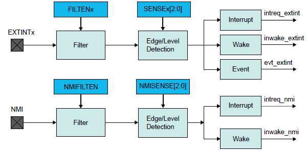
Second, handling reading data with an external pin change interrupt. From my examination of the datasheet, it appears there’s only a single interrupt vector for external interrupts, and the interrupt handler must examine another register to determine which pins actually triggered the interrupt. That means the same handler must not only check the signals described above for reading data, but also other signals that require interrupt handling, like writeRequest (used when the computer writes to the disk) and multiple enable signals (used to select one of several disks that may be present).
bool driveEnabled = false;

EIC_Interrupt_Handler()
{
	if (EIC_INTFLAG & ENABLE_PIN_MASK)
	{
		// enable input has changed
		EIC_INTFLAG &= ~ENABLE_PIN_MASK; // clear interrupt
		driveEnabled = (PIN_STATE & ENABLE_PIN_MASK);
		if (driveEnabled)
			PIN_MODE_OUTPUT_ENABLE |= R_PIN_MASK;
		else
			PIN_MODE_OUTPUT_ENABLE &= ~R_PIN_MASK;
	}

	if (driveEnabled)
	{
		if (EIC_INTFLAG & WRITE_REQUEST_PIN_MASK)
		{
			// writeRequest input has changed
			EIC_INTFLAG &= ~WRITE_REQUEST_PIN_MASK; // clear interrupt
			writeState = (PIN_STATE & WRITE_REQUEST_PIN_MASK);

			// set status flags here to handle beginning and ending
			// of disk sector writes in the main loop
		}

		if (EIC_INTFLAG & ADDR_PINS_MASK)
		{
			// the A3..A0 input pins have changed
			EIC_INTFLAG &= ~ADDR_PINS_MASK; // clear interrupt
			registerNumber = ((PIN_STATE & ADDR_PINS_MASK) >> ADDR_PINS_SHIFT); // get A3..A0

			if (internalState[registerNumber])
				PIN_OUTPUT_VALUE |= R_PIN_MASK; // set R to 1
			else
				PIN_OUTPUT_VALUE &= ~R_PIN_MASK; // set R to 0

			if (registerNumber == INSTANTANEOUS_DISK_DATA_REGISTER)
				PIN_MUX[R_PIN] = PERIPHERAL_SPI;
			else if (registerNumber == MOTOR_TACHOMETER_REGISTER)
				PIN_MUX[R_PIN] = PERIPHERAL_TIMER_COUNTER;
			else
				PIN_MUX[R_PIN] = GPIO;
		}
	}
}
There’s some extra code about enable and write request. For the address, the interrupt handler must also adjust the mcu’s pin mux to control what’s actually driving the output on the R pin. In most cases it’s a GPIO, and the value comes from the internalState[] array and is set in the PIN_OUTPUT register. But for some addresses, the selected value is a dynamically changing quantity that comes from an active SPI peripheral, or a timer/counter peripheral.
Interrupt Priority and Pre-emption
EIC_Interrupt_Handler should be given the highest interrupt priority, higher than interrupts for other events like button pushes or SD card data transfers. With a higher priority, I’m fairly certain the EIC_Interrupt_Handler will interrupt any other interrupt handler that might be running at the time. Isn’t that what’s meant by the “nested” part of the ARM’s nested vector interrupt controller?
What about the PCC_Interrupt_Handler, for writing data? Should it have the same priority, or a lower one? Should reads interrupt writes? Can that ever actually happen? Does it matter? I’m not sure.
Can the EIC_Interrupt_Handler interrupt itself? If A0 changes, and EIC_Interrupt_Handler begins to run, and then A1 changes, will the handler be interrupted by a second invocation of the same handler? I think the answer is no. But what probably happens is that the interrupt flag will be set again, and as soon as EIC_Interrupt_Handler finishes, the interrupt will trigger again and EIC_Interrupt_Handler will run again. That seems inefficient, but it’s probably OK.
Interrupt Timing
Now we come to the critical question: can EIC_Interrupt_Handler respond to changes on A3..A0 with a new value on R within 500ns?
My research suggests the answer is maybe, but it will be difficult. I found two discussion threads where people were attempting to do something similar with Atmel SAM Cortex M4 and M7 microcontrollers. The first used a 300MHz SAME70, and found a 300ns latency to the start of the interrupt handler. The second used a 120 MHz SAM4E and found a 200ns latency to the start of the handler. These are the delays from the input pin transition to when the interrupt handler begins to run, and they don’t include the actual execution time of the interrupt handler, which is probably several hundred nanoseconds more.
Why so slow? First, the Cortex M4 has a built-in interrupt latency of 12 clock cycles. That’s to do whatever the hardware does for interrupt processing – save the execution state, fetch the interrupt vector, and whatever other voodoo is required. At 120 MHz that’s already 100ns gone.
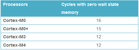
Then the first instruction of the interrupt handler code must be fetched from internal flash memory. At 120 MHz, the flash isn’t fast enough to supply data in a single clock cycle. It requires 5 wait states, so a read from flash memory needs 6 total clock cycles. That’s another 50ns. So even in the theoretical best-case performance, it will still be a minimum of 150ns before the interrupt handler can begin to run. The two real-world examples I mentioned above were slower.
What about these flash wait states? Does it mean that every instruction in the interrupt handler will need 6 clock cycles to load from flash? I don’t understand the details, but the answer is no. There’s some prefetching and caching happening. Also most instructions are 16 bits wide, and the flash has a 128 bit width, so several instructions can be prefetched and cached at the same time. At least for straight line code with no jumps, I’m guessing that the rest of the interrupt handler can run at speeds approaching 1 instruction per clock cycle at 120 MHz. If anybody knows of good reference data for this, please let me know.
If the flash wait states are a major problem, it may be possible to copy the interrupt handler code to RAM and run it from there. I’m assuming the internal RAM has zero wait states, but I might be wrong on that point.
So 150ns before the interrupt handler can begin to run leaves 350ns remaining. That’s 42 clock cycles at 120MHz. So the interrupt handler can be up to 42 instructions long, on its longest execution path? Not quite, because some common instructions like STR require two clock cycles. Assuming an average time of 1.5 clock cycles per instruction, those 42 clock cycles are only enough for 28 instructions. Can EIC_Interrupt_Handler be implemented in only 28 Thumb assembly instructions? Um… maybe?
Complicating Factors
A few other factors raise the difficulty bar further. If the main code ever disables interrupts, or performs any atomic operations, it will delay running of the EIC_Interrupt_Handler and cut further into that 500ns window. In code that uses lots of interrupts, sometimes it’s impossible to avoid needing critical sections where interrupts are briefly disabled, for example to check some value and then set another value based on the first one. Failure to do this can cause rare but serious bugs, if an interrupt intervenes between reading the first value and setting the second.
Another serious complication is the possibility of multiple back-to-back invocations of EIC_Interrupt_Handler. What happens if one of the A3..A0 inputs changes immediately after execution of the line:
registerNumber = ((PIN_STATE & ADDR_PINS_MASK) >> ADDR_PINS_SHIFT); // get A3..A0
The remaining code will output the value of R for the old A3..A0, then the interrupt handler will finish, then a new interrupt will trigger and the handler will be invoked again to process the new A3..A0 input state. The total latency from the change on A3..A0 to the final correct output value of R will be something like 1.5 times the latency for the normal case. In a system where the timing margins are already very tight, that may be enough to break it entirely.
I don’t see any way around this back-to-back invocation problem. Moving EIC_INTFLAG &= ~ADDR_PINS_MASK to the end of EIC_Interrupt_Handler wouldn’t help anything. It would actually clear the pending interrupt flag from the second change of A3..A0 without ever responding to it, resulting in incorrect behavior.
Conclusions
So can this work – is software interrupt processing viable with these kinds of timing requirements? Is there some optimization trick I can use in the interrupt handler to improve things? Should I even spend the time to attempt it? Maybe there’s some clever way to use the built-in CCL programmable logic that I’ve overlooked, to help accelerate the interrupt handler or even replace it entirely? Or should I just write off this idea as too difficult and too problematic, and continue using a separate programmable logic chip for a mux and glue logic? Decisions…
Read 15 comments and join the conversationAtmel-ICE + Floppy Emu. The Taste of Sadness
In all the time I’ve been developing Floppy Emu, can you believe I’ve never had a debugger? I use the Atmel AVRISP mkII to program the Emu’s ATMEGA1284 microcontroller, but the mkII only supports programming and not debugging. I don’t have a serial port or other logging mechanism either, so when I encounter mystery problems, I need to debuga them by displaying one-time error codes or blinking an LED. Not very convenient.
Last week I finally purchased a proper debugger – the Atmel-ICE. It supports both JTAG and debugWIRE debugging, which are the two interfaces used in the ATMEGA family of microcontrollers. The Atmel-ICE also supports Atmel’s SAM family of 32-bit ARM microcontrollers, which will be handy if/when I start working with those.
With excitement, I connected the Atmel-ICE to Floppy Emu’s 6-pin ISP port. I was able to communicate with the ATMEGA1284 chip, view its fuses, and reprogram it. Visions of breakpoints and memory dumps danced in my head – this was going to be awesome. Then I started a debug session, only to encounter this error:
Use Start Without Debugging to avoid this message.
Wha-wha-what? Does not support debugging??
I searched in vain for a debugWIRE option, but the only interface choices displayed by the software were ISP and JTAG. After a frantic documentation search I discovered the sad truth. I’d thought the ATMEGA1284 had both debugWIRE and JTAG debugging interfaces, but the presence of JTAG actually means the chip doesn’t support debugWIRE. Even though the necessary debugWIRE pins are right there, and debugWIRE is mentioned in the chip’s datasheet, and there’s a debugWIRE enable fuse on the chip. Ugh.
I confirmed that a test project configured for the ATMEGA328P causes the debugWIRE option to appear in the Atmel Studio software. But Floppy Emu doesn’t have a ATMEGA328P. As soon as I change the project’s device type to ATMEGA1284, the debugWIRE option disappears.
Unfortunately I can’t use the JTAG interface, because I didn’t plan for it, and there’s no JTAG connector on the Floppy Emu board. I can’t do micro-soldering surgery to create a JTAG port either, because the ATMEGA1284 JTAG pins are connected to the board’s Xilinx CPLD chip, to support runtime reprogramming of the CPLD.
I’ll continue debugging with a blinking LED. Debuggers are for wimps. 🙂
Read 2 comments and join the conversationThoughts on Floppy Emu Redesign

I’ve been pondering what a redesigned Floppy Emu might look like – what ICs might be involved. So why mess with success? The current design combines a microcontroller with a CPLD, which has proven to be a powerful and flexible combination. But the specific microcontroller and CPLD that I chose have both become a bit outdated, hard to find, and too expensive relative to the alternatives. By replacing them both with more modern parts, I could probably gain better features while simultaneously improving the manufacturing outlook, for a perfect win/win. Or with a sufficiently powerful microcontroller, I might be able to completely eliminate the CPLD.
CPLD
The CPLD (complex programmable logic device) is like a miniature FPGA, and is there to handle the timing-critical bit twiddling that the microcontroller can’t. It ensures the data bitstream appears at exactly the right speed, with no jitter, and also functions as a fancy parallel-to-serial shift register. For Apple II disk emulation, it helps make the work easier, and for Macintosh disk emulation it’s essential. The Mac treats floppy drives sort of like a 16×1-bit external memory, and microcontroller software isn’t fast enough to react to the changing address inputs and supply the correct data output.
The specific CPLD used by Floppy Emu is the Xilinx XC9572XL, which I mainly chose for being 5v tolerant. It works, but it can only store a very small amount of logic, which forces me to have separate and independent firmwares for Apple II and Macintosh emulation. With a larger and more capable chip, I could merge those into a single firmware.
The Xilinx XC9572XL is old enough that it’s approaching “legacy” status, and may be in line for discontinuation soon. Xilinx barely mentions it on their web site, and the chip has been sold out at all of their distributors for the past several weeks, which is worrisome. During the years I’ve been building Floppy Emus, the price of the XC9572XL has also steadily climbed to where it’s now more than double its original cost.
There aren’t many great alternatives, because it seems the whole CPLD market is slowly dying in favor of FPGAs, and most of what’s left has even smaller logic storage limits than the XC9572XL. The best option is probably a small FPGA instead, like one of the Lattice MachXO or MachXO2 devices similar to what’s in the Yellowstone disk controller.
A second idea is to replace the CPLD with a small, dedicated microcontroller, like something from the ATTINY series. With only one or two very simple tasks to do, maybe a mini-microcontroller would be able to keep up. I spent half a day pursuing this line of thinking, going as far as writing a first draft of the code for this hypothetical microcontroller, but decided to focus on other solutions first.
Microcontroller
Floppy Emu uses an ATMEGA1284 microcontroller, which in 2018 is almost a joke. Its sole advantage is that it’s a close relative of the ATMEGA chip used in Arduinos, so there’s tons of example code available for it. But it’s woefully underpowered compared to basically any other microcontroller out there. Any of the popular 32-bit ARM microcontrollers would have significantly faster clock speeds, more memory, and better peripheral options, and would probably cost less too.
Sadly there are still no common microcontrollers with enough internal RAM to buffer an entire floppy disk image (140K to 1440K depending on the image type). That would vastly simplify the emulation, help fix some occasional emulation hiccups, and possibly lead to better handling of copy-protected disks. But that will have to wait until the 2020’s, it seems.
After looking at a whole range of options, I’ve got my eye on the Atmel SAM4S series of microcontrollers. These boast speeds up to 120 MHz, while remaining relatively inexpensive.
Single-Chip Design?
Earlier I mentioned that the CPLD is essential for certain types of disk emulation, where microcontroller software isn’t fast enough to react to changing inputs in real time. That’s true for an older 8-bit microcontroller like the ATMEGA1284 running at 20 MHz, but what about for a modern 32-bit ARM running at 120 MHz? That might be a different story.
The hardest test will be 3.5 inch floppy disk emulation for the Macintosh. When the Mac wants to check some item of drive state, like whether there’s a disk inserted or whether the disk head is at track zero, it sets four IO lines with the right values to select from among the 16 possible state bits. Then it reads the result on a fifth IO line. It works just like an asynchronous SRAM, and the drive (or Floppy Emu emulating a drive) never knows if or when the Mac is reading state info. The drive needs to constantly respond, so whenever one of those four IO lines changes, the value on the fifth IO line must be updated immediately to reflect the newly selected state.
This would be difficult to emulate in a microcontroller, especially if it also needed to do other work besides merely responding to changing address inputs. The microcontroller would need to enable a pin change interrupt on each of the four address lines, and the interrupt service routine would need to read the address lines and set the data line accordingly. In practice it would be even more complicated, because there are other IO lines like /ENABLE that would also need to be considered, and would need their own interrupt handlers.
Would it be fast enough? Maybe. By itself the code in the ISR would almost surely be fast enough. But there’s overhead to consider – the interrupt service latency, and the time needed to set up the ISR context and exit it again (saving and loading all the registers from the stack). Then there’s the complicating factor of other potential interrupts, or other invocations of this same interrupt, creating additional delays before the ISR actually starts running. And the further complication of some critical code sections where interrupts need to be disabled temporarily, creating yet more delays before the ISR runs.
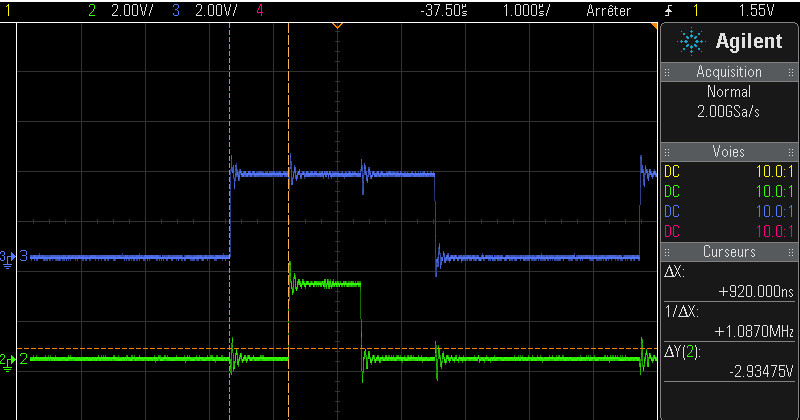
How fast does it need to be, anyway? How much time elapses between when the Mac sets the four IO lines and when it reads the fifth line? Unfortunately I don’t know, and the worst part is there’s really no way to find out. Because there’s no external indication of when a read is occurring, there’s nothing I can measure with an oscilloscope or logic analyzer. But I can make some rough guesses, based upon examination of a disassembly of the floppy disk driver code in the Macintosh ROM. On the Macintosh Plus, there’s a whopping 6750 ns between address and data for most state reads, but some reads have a much narrower window of about 1500 ns, assuming I’ve interpreted the code correctly.
Are there other faster read examples, buried somewhere in the Mac Plus ROM that I missed? And do Macs with a higher clock speed than the Plus have correspondingly faster read behaviors of disk state info, or do they insert delay code to keep the speed constant? I don’t know, but the Mac Plus is likely far from the worst case. I’ll make a wild guess that a 500 ns response time would probably be fast enough. Keep in mind I’m talking about the speed between presentation of the four address IO lines, and reading state info on the fifth IO line, which is entirely different from the speed or data rate of the disk data itself. It’s not something that’s specced or defined in any official source; it’s just something that arises as a side-effect of the code in the Mac’s ROM.
Despite the uncertainty here, I think there’s a decent chance this could work, so I’m going to try some experiments to test my theories.
If even a 120 MHz microcontroller isn’t fast enough to handle this 4-address-1-data mechanism, I’ve sketched out a possible fallback plan that uses a few discrete logic chips – some muxes and latches and buffers. It’s arguable whether that would be preferable to just using a CPLD (or FPGA), and it would certainly be less flexible. But a small handful of discrete logic combined with a much faster microcontroller could still provide some major advantages, and simplify firmware design by reducing the number of programmable chips on the Emu board from two to one.
So there’s a lot to think about. And anything that grows out of all this ruminating won’t see the light of day for a long time. But I can’t resist daydreaming…
Read 18 comments and join the conversationGarbage In, Garbage Out
I’m beginning to suspect there’s something subtly wrong with my Apple IIe, which might explain a lot of strange intermittent errors I’ve recently observed with Yellowstone and Floppy Emu development. It’s hard to know what to conclude, but when you can’t trust your test equipment, it’s impossible to trust the validity of your test results.
Recently I used this Apple IIe to test my new Floppy Emu OLED prototype board. When connected to a standard Apple Disk 5.25 controller card, everything worked fine initially. But when I tried doing some ProDOS file copy operations, the Floppy Emu spontaneously reset to the happy face / self-test screen. DOH! I tried it twice, and the Emu reset itself during the copy operation both times. I concluded there must be something wrong with the prototype board.
Then I tried the copy test two more times, and got different results. The Emu prototype didn’t reset itself, but the OLED display went blank several times during the copy operations. Hmmm.
So then I tried a plain vanilla Floppy Emu Model B, the same hardware and firmware that I’ve been using successfully for more than a year. I found that when trying to boot the Apple IIe from a ProDOS v1.9 disk image, the Model B’s LCD went blank several times during booting. Huh? This happened in two consecutive test runs, but then mysteriously stopped happening. I also tried the same file copy operations I’d done with the OLED prototype board, and saw a similar behavior where the LCD went blank a few times during the copy. But as before, after reproducing the bug twice in a row, it stopped happening.
Finally I went back to the OLED prototype board, and this time everything worked fine. No more unexplained resets or display blank-outs.
Maybe there’s something wrong with the Apple IIe’s power supply, or some problem where it needs to warm-up for a while before it works reliably? My first OLED prototype board tests were the first time I’d powered on the Apple IIe in several days, so it was cold. During an hour of testing, the strange Floppy Emu problems I’d observed gradually disappeared. It doesn’t really make sense to me, but it’s the best explanation I can think of. This might also explain some strange unexpected resets of the Floppy Emu last month, when I tested it with the Yellowstone card. In fact, it casts doubt on all of my Yellowstone testing.
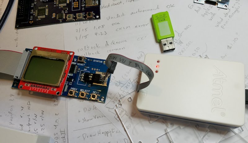
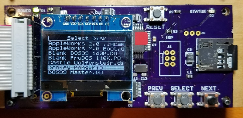
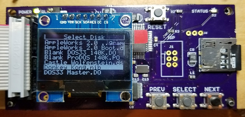
Read 9 comments and join the conversationFloppy Emu OLED Prototype

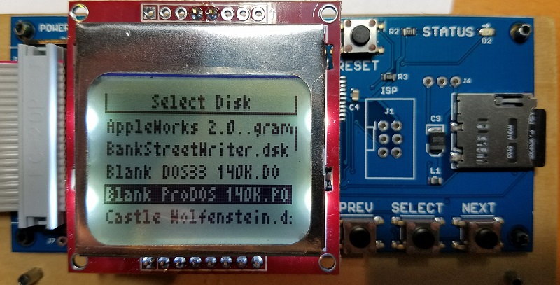
Displays, displays! I’ve built a prototype Floppy Emu board that uses a 1.3-inch 128×64 OLED display, instead of the existing 1.4-inch 84×48 LCD. It works, and it looks very nice. So is this the answer to my display worries? Take a look at the photos, and tell me what you think.
Why change displays? The current edition Floppy Emu uses an 84×48 LCD that’s a clone of the Nokia 5110 mobile phone display. It’s a decent module with a nice built-in backlight, but the displays have caused me a lot of headaches over the years due to their iffy quality control. Around 10-15% are dead on arrival and must be discarded during manufacturing and testing. A large fraction of the remainder exhibit flaky behavior until the LCD’s pressure-fit connector is manually fine-tuned. These LCD hassles consume too much of the manufacturer’s time and my time. The supply chain for the 5110 LCDs is also problematic, coming only from small eBay and Aliexpress sellers, instead of a major manufacturer who can provide documentation and support.
Last month I reviewed some potential replacement displays. There weren’t many great options, but after lots of consideration I settled on this 1.3-inch OLED. It’s similar to the 5110 LCD in many ways, being a 1-bit graphical display with an SPI interface. The physical size is a bit smaller than the 5110 LCD, but they’re close. Unfortunately the supply chain situation for the OLED is even worse than the 5110 LCD, and the cost is at least $2 more per unit. But if I can save myself $2 worth of hassle, it will be worth it. A few weeks ago I hacked up a Floppy Emu board to support the OLED, just to prove that it worked, and today I now have a proper OLED Emu prototype.
I For One Welcome Our New OLED Overlords
The first thing you’ll notice about the OLED is that the contrast is amazing. The display is bright and very crisp, and the photos can’t do it justice. I never thought the 5110 LCD looked bad, but the OLED looks far superior.
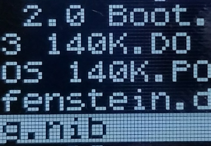
The extra resolution of the OLED helps a lot. Text characters on the 5110 LCD are 3×6, while on the OLED they’re 5×7. This makes possible a more finely-detailed font that’s a nice improvement in legibility.
Text on the OLED is smaller, and at first I was concerned this would make it difficult to read. But with the awesome contrast and better font, my weak eyes find the OLED to be about equally easy to read as the larger text on the 5110 LCD. My wife declared the OLED more readable than the 5110 LCD. The OLED text is also larger than the text on my Backwoods Logger Mini (2011 flashback alert), and is about the same size as this CorelDRAW quick reference card I happened to have sitting out:
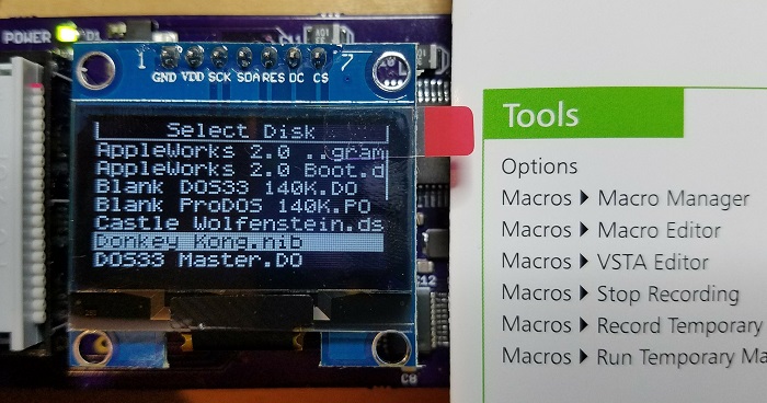
The OLED shows eight rows of text, compared to six rows on the 5110 LCD. This is a nice bonus when scrolling through a long list of filenames. With some extra development work and possible resulting display update slowness, future firmware might be able to trade fewer rows for larger text, but the OLED is designed around eight rows in hardware.
Fun with Fonts
I tried two different fonts. The first font has most letters being 5×6 pixels, with only the descenders of g, j, p, q, and y dropping below the baseline to make a 5×7 letter. Since each row is 8 pixels tall, the 5×6 letters provide two pixels of whitespace between rows. Here’s a sample:
The second font has most letters being 5×7 pixels. There are no true descenders, so g, j, p, q, and y sit on the same baseline as all the other letters. Because the letters are one pixel taller, this font is slightly more detailed and more readable than 5×6. But with only a single pixel of whitespace between rows, the text looks sort of cramped. I decided I didn’t like it, but maybe you’ll feel differently. Here’s a sample:
For comparison, here is the 3×5 font on the 5110 LCD:
Now What?
So it works. Now what? If I want to move forward with this OLED, there’s a lot of work to do. I need to find a supplier who can reliably provide hundreds of these displays. I need to get my updated PCB to my manufacturing partner. Because it’s a new design, I’ll have to pay them a bunch of money for one-time engineering fees. I’ll need to update the manufacturing instructions, and the test procedure, and the firmware that goes with it. And I’ll need to design a new case to fit the new board and OLED. It will all be a lot of work, and when it’s done my costs will have increased by $2 per unit. Is the pain worth it? Probably yes, but I’m still undecided.
I might do some experiments with another display I recently discovered, this COG 12864 LCD. It’s a little bigger than the OLED, which might be helpful, but it lacks the OLED’s excellent contrast and crispness. Its resolution is the same as the OLED, and it’s roughly the same price, and the manufacturing work needed to change displays would still be the same. I’m not sure there’s a compelling reason to choose the COG 12864 LCD over the OLED, but it’s a similar contender. Hmmm.
Of course the best option might still be to do nothing, and keep the 5110 LCD. Yes it’s a headache, but it’s a headache I’m familiar with and have dealt with successfully for four years. A new display would bring its own set of headaches through required manufacturing changes and case redesign, so I’m going to have headaches no matter what! But when I think about the best long-term solution, I’m drawn to the idea of a more reliable, better looking OLED.
Enjoy some gratuitous unnecessary zoom: