

Archive for the 'Dev Tools' Category
Rigol DS1074Z Oscilloscope Review
Here’s my long-overdue review of the Rigol DS1074Z four-channel oscilloscope, which I purchased a couple of months ago. At around $550, the DS1074Z occupies a unique place in today’s oscilloscope market between the $300 entry-level scopes, and the $850+ higher end scopes like Rigol’s new DS2000 series. It’s also one of the only scopes in this range to offer four channels.
I felt a little unprepared to do a review, since during the time that I’ve had the scope, I’ve really only scratched the surface of its features. If there’s something not covered in the video or something else you’d like me to test, leave me a note in the comments. A quick summary of what’s covered in the video:
Likes – display, menus, measurement features, memory size, SPI decoding
Dislikes – fan noise
If you’re shopping for a new oscilloscope and can stretch your budget beyond the entry-level choices, the DS1074Z is definitely worth a look.
Read 13 comments and join the conversationCortex M3 For Dummies – STM32 Discovery Board

The ARM Cortex M3 has generated lots of buzz lately. Maybe you’ve been working with Arduinos, AVRs, or PICs for a while, and heard about the Cortex M3, but weren’t sure what it was all about or whether it was even relevant to you. This review will try to shed some light on the Cortex M3’s capabilities and development tools, using the STM32VLDiscovery board from ST Microelectronics.
The nice folks at Newark sent me a STM32VLDiscovery Cortex M3 evaluation board for review. This little board packs a big bunch for a remarkably low price. It can be found for under $10 if you hunt around for a deal, which is an amazing value. ST is also currently running a promotion in which residents of the USA and Canada can get a free STM32F4Discovery board, which is similar to the board reviewed here.
Although the STM32 Discovery board isn’t marketed as an Arduino competitor, it could be one. Its size, layout, and functionality make it a reasonable replacement for many applications needing a small microcontroller board with lots of I/Os for experiments and mad scientist projects. To help put its specs into context, I’ve selected a few other boards that readers may be familiar with for comparison purposes. All the boards contain a microcontroller along with one or two buttons and LEDs, with I/Os connected to hobbyist-friendly 0.1 inch headers, and can be programmed with a plain USB cable. In addition to the STM32 Discovery, they are the Arduino Uno, Arduino Mega 2560, and Copper AVR32.
| STM32VL Discovery | Arduino Uno | Arduino Mega 2560 | Copper AVR32 | |
| Price | $10 | $25 | $50 | $38 |
| Processor | STM32F100 Cortex-M3 | ATmega328P AVR | ATmega2560 AVR | AT32UC3B1256 AVR |
| Type | 32 bit | 8 bit | 8 bit | 32 bit |
| Flash (KB) | 128 | 32 | 256 | 256 |
| EEPROM (KB) | 0 | 1 | 4 | 0 |
| RAM (KB) | 8 | 2 | 8 | 32 |
| Max Speed (MHz) | 24 | 20 | 16 | 60 |
| Voltage (V) | 2.0 – 3.6 | 1.8 – 5.5 | 1.8 – 5.5 | 3.0 – 3.6 |
| User I/O Pins | 51 | 20 | 70 | 28 |
| SPI channels | 2 | 2 | 5 | 3 |
| I2C channels | 2 | 1 | 1 | 1 |
| UART channels | 3 | 1 | 4 | 2 |
| ADC channels | 16 | 8 | 16 | 6 |
| DAC channels | 2 | 0 | 0 | 0 |
| USB | no | no | no | yes |
The table makes it clear that you’re getting a lot of microcontroller for your money. ST is very likely selling these boards at a loss, because their goals are different than the makers of the other boards. ST isn’t trying to sell you a prototyping product, but rather they’re trying to get you familiar with their line of STM32 microcontrollers so you’ll go on to incorporate them into a product of your own design. To appreciate this, it’s necessary to understand the ARM Model that gave rise to the Cortex M3.
The ARM Model
The Cortex M3 and other ARM processors were designed by ARM Holdings, a British semiconductor company. ARM doesn’t actually manufacture the processors they design, but instead they license the designs to other semiconductor companies, who then turn them into specific chips and sell them under their own brand names. Thus ST’s STM32 line of microcontrollers, Texas Instruments’ Stellaris line, NXP’s LPC1000 line, Atmel’s AT91SAMxx line, and many others are all Cortex M3 microcontrollers. All use the same instruction set, and have very similar features, so you could find a chip in any of those lines that’s a near functional equivalent of the STM32F100RB chip on the Discovery board. The chips aren’t exact clones, however. They differ in the amount of on-chip memory, clock speeds, pin configuration, peripheral units, and other features.
Unfortunately this is the Cortex M3’s biggest obstacle to gaining more traction in the electronics hobbyist community, because there isn’t really a “Cortex M3 community”. There’s a Stellaris community, and an LPCxxxx community, and an STM32 community, and so on. Each one is just different enough from the others to make manufacturer-independent tools and code sharing difficult. By fracturing the community into many different parts, it also makes it harder for it to reach a critical mass necessary to catch significant public interest in the way AVR and PIC have.
ARM Cortex M3
So what exactly is a Cortex M3? It’s a microcontroller, like an AVR or PIC. That means it has built-in Flash memory and RAM, lots of general-purpose I/O pins that can be controlled individually through software, and built-in peripherals for things like serial communication or analog-to-digital conversion. Where the Cortex M3 differs from 8-bit AVRs and PICs is that it’s a 32-bit processor, capable of running at speeds up to 100 MHz in some versions, and is a cousin of the higher-end ARM processors found in devices like Apple’s iPad and in some PCs. It also offers larger memories than typically found on AVR or PIC microcontrollers. In short, it’s like a beefed-up version of the micrcontroller you’re using now.
A few interesting features of the Cortex M3 aren’t found on typical 8-bit microcontrollers, like hardware divide support, an internal PLL for clock synthesis, and two digital to analog converters. The M3 also has a clever remappable pin feature, which lets you choose from among several options for which pins to use for I2C, SPI, USART, ADC, and other hardware units. This provides extra flexibility in board design and port usage.
The Cortex M3 has a newer sibling called the Cortex M0. The M0 is geared towards lower cost, lower power applications than the M3, but the two are very similar. Most of what you read about the M3 on the web also applies to the M0.
While it has arguably generated the most buzz lately, the Cortex M3 is by no means the only entry in the 32-bit high performance microcontroller market attempting to supplant 8-bit mcus like the AVR ATmega. Another example is the AVR32 chip, found on the Copper board. This 32-bit microcontroller is also made by Atmel, although it shares little with Atmel’s 8-bit microcontrollers beyond the AVR name.
The STM32VLDiscovery Board
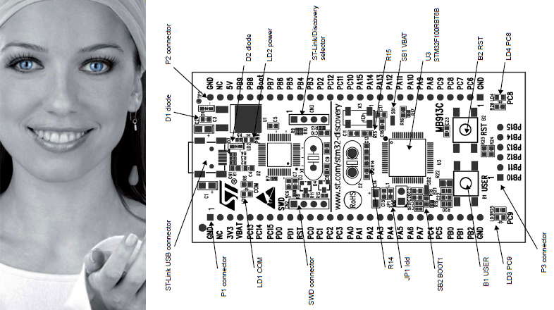
ST’s name for their Cortex M3 product line is STM32, and the STMVL32Discovery board is the smallest and least expensive of their Cortex M3 evaluation boards. Now who is this woman that appears on all of ST’s marketing materials for the STM32 line? Her photoshopped eyes look a bit disturbing. Some of their STM32 materials also use a rainbow-colored butterfly logo, which I like much better.
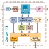
The STMVL32Discovery board is actually two boards in one: everything to the left of the vertical line in the above diagram is an ST-Link programming/debug module. It can be used with the Cortex M3 module on the right side of the board, or to program and debug a STM32 mcu on another board in a stand-alone application that lacks a programmer. I believe an earlier version of the ST Discovery board actually had perforations in the PCB so you could break-off the ST-Link module and use the two halves separately, but with the STMVL32Discovery there’s only a line in the silkscreen to remind you there are two functionally separate modules on a single board.
At roughly 3.3 x 1.7 inches, the board is smaller than a standard-size Arduino. Two rows of 0.1 inch header down the sides of the board make it easy to connect other components. The headers are on both the top and the bottom of the board, so you can make connections from either side, which is a nice touch. You could almost drop the ST Discovery right into a breadboard, except for the 6-pin header along its right edge. I’m not sure what ST was thinking here, because when inserted into a breadboard, these six pins will all be tied together in a single row. Depending on the layout of your breadboard, you may be able to insert the ST Discovery such that those six pins hang off the edge, unconnected.
Besides the Cortex M3 itself, the board also contains two user-controllable LEDs, a user push button, and a reset button. That’s similar to what you’ll find on an Arduino board, and is just enough to test things out and make sure it’s all working before connecting more components.
The board is powered over USB, or optionally from an external supply. When first connected to your PC, it immediately runs a demo program that flashes the LEDs in different patterns when you press the user push button. Under Windows it also automatically mounts itself as a read-only USB storage drive, which contains a few files with links to the online documentation. That’s pretty slick.
There’s no printed documentation included with the ST Discovery board, but the online user manual is quite well done. It includes a quick-start guide, block diagram, layout diagram, mechanical drawing, full schematics, explanation of all the jumpers and solder bridges, and a pin description table. The companion software package includes the libraries and header files for ST’s version of the Cortex M3 and for the ST Discovery board peripherals, as well as several example projects. On ST’s web site you’ll also find detailed tutorials for building and running the example projects using the three officially supported development toolchains.
ARM Development Tools

There are a bewildering number of development toolchain choices for ARM Cortex M3 development. It’s hard to overstate just how painful this makes the getting started process for a beginner. Worse still, the only officially-supported toolchains (IAR, Keil, and Atollic) are professional tools which are very expensive, and certainly won’t be of interest to any hobby developers. When their web page has a “get a quote” link instead of listing an actual price, that’s the clue to look elsewhere. For reference, the Keil tools cost $4895 for a single license, and the others are similar. Ouch!
The professional tools do all offer a time-limited trial version or a code size-limited version, but few hobbyists will be happy with those as a permanent solution.
If you’re willing to cough up a little money (but not $4895) for a well-made development tool with good support, Rowley Associates Crossworks is well-regarded and is just $150 for a personal license.
After looking at more than a dozen different development tools, I decided to put together my own toolchain based on the CodeSourcery CodeBench g++ Lite GNU command line tools and Eclipse C/C++ IDE. This excellent setup guide for Eclipse and CodeSourcery with STM32 describes the process in detail, so I won’t list all the setup steps here. Depending on your familiarity with other development environments and your tolerance for this sort of job, you may find the process anywhere from slightly tedious to completely impossible. It involves installing Eclipse, the Java runtime, CodeSourcery, GDB server, the STM32 SDK, and the ST-Link programming utility from six different sources, and then configuring them all to work together properly. It really makes you appreciate the convenience of a tool like Atmel’s AVR Studio, which performs all of the same functions in a single tool with a single download and install process. All together, it took me about 90 minutes to get the STM32 Cortex M3 development tools configured and program one of the example projects onto the ST Discovery board.
Cortex M3 Software Development
OK, let’s blink some LEDs. Here’s the simplest of the examples provided by ST:
#include "stm32f10x.h"
#include "STM32vldiscovery.h"
GPIO_InitTypeDef GPIO_InitStructure;void Delay(__IO uint32_t nCount);int main(void) { /* Configure all unused GPIO port pins in Analog Input mode (floating input trigger OFF), this will reduce the power consumption and increase the device immunity against EMI/EMC *************************************************/ RCC_APB2PeriphClockCmd(RCC_APB2Periph_GPIOA | RCC_APB2Periph_GPIOB | RCC_APB2Periph_GPIOC | RCC_APB2Periph_GPIOD | RCC_APB2Periph_GPIOE, ENABLE);GPIO_InitStructure.GPIO_Pin = GPIO_Pin_All; GPIO_InitStructure.GPIO_Mode = GPIO_Mode_AIN; GPIO_Init(GPIOA, &GPIO_InitStructure); GPIO_Init(GPIOB, &GPIO_InitStructure); GPIO_Init(GPIOC, &GPIO_InitStructure); GPIO_Init(GPIOD, &GPIO_InitStructure); GPIO_Init(GPIOE, &GPIO_InitStructure);RCC_APB2PeriphClockCmd(RCC_APB2Periph_GPIOA | RCC_APB2Periph_GPIOB | RCC_APB2Periph_GPIOC | RCC_APB2Periph_GPIOD | RCC_APB2Periph_GPIOE, DISABLE);/* Initialize Leds LD3 and LD4 mounted on STM32VLDISCOVERY board */ STM32vldiscovery_LEDInit(LED3); STM32vldiscovery_LEDInit(LED4);while (1) { /* Turn on LD2 and LD3 */ STM32vldiscovery_LEDOn(LED3); STM32vldiscovery_LEDOff(LED4); /* Insert delay */ Delay(0xAFFFFF);/* Turn off LD3 and LD4 */ STM32vldiscovery_LEDOff(LED3); STM32vldiscovery_LEDOn(LED4); /* Insert delay */ Delay(0xAFFFFF);} }void Delay(__IO uint32_t nCount) { for(; nCount != 0; nCount--); }
If you’ve previously developed software for other microcontrollers, then this probably looks fairly understandable. The first step is to configure all of the I/O pins as inputs, akin to setting the DDR (data direction) register on an AVR or calling pinMode() with the Arduino environment. In this case, the I/Os are configured by passing a struct to a function instead of directly twiddling some bits in a register, although it’s likely that the implementation of GPIO_Init() does something like that under the hood. That RCCABP2PeriphClockCmd() function looks a little strange, though– it appears the port’s clocks need to be explicitly enabled before configuration, then disabled afterwards.
The rest is just manipulation of the LEDs, but it’s a bit more abstract than most people are probably accustomed to seeing. You don’t normally need to initialize an LED or call a function to turn it on. These functions are provided by the ST Discovery board library to simplify development, but curious minds will want to know what they actually do. Here’s the implementation of STM32vldiscovery_LEDInit() and definitions of LED3 and LED4:
typedef enum
{
 LED3 = 0,
 LED4 = 1
} Led_TypeDef;
const uint32_t GPIO_CLK[LEDn] = {LED3_GPIO_CLK, LED4_GPIO_CLK};#define LED3_GPIO_CLK RCC_APB2Periph_GPIOC #define LED4_GPIO_CLK RCC_APB2Periph_GPIOCvoid STM32vldiscovery_LEDInit(Led_TypeDef Led) { GPIO_InitTypeDef GPIO_InitStructure; /* Enable the GPIO_LED Clock */ RCC_APB2PeriphClockCmd(GPIO_CLK[Led], ENABLE);/* Configure the GPIO_LED pin */ GPIO_InitStructure.GPIO_Pin = GPIO_PIN[Led]; GPIO_InitStructure.GPIO_Mode = GPIO_Mode_Out_PP; GPIO_InitStructure.GPIO_Speed = GPIO_Speed_50MHz; GPIO_Init(GPIO_PORT[Led], &GPIO_InitStructure); }
So STM32vldiscovery_LEDInit() enables the clock for port C, where the LEDs are connected, and then configures the correct pin in port C as an output. GPIO_Mode_Out_PP specifies a push-pull output, in other words a normal output that’s actively driven high and low. GPIO_Speed_50MHz controls the rise and fall times of the output signal. Selecting a faster speed will produce shorter rise and fall times, but will consume more current and generate more supply voltage swings and electrical noise.
Lastly, let’s take a look at STM32vldiscovery_LEDOn() and STM32vldiscovery_LEDOff():
void STM32vldiscovery_LEDOn(Led_TypeDef Led)
{
    GPIO_PORT[Led]->BSRR = GPIO_PIN[Led];
}
void STM32vldiscovery_LEDOff(Led_TypeDef Led) { GPIO_PORT[Led]->BRR = GPIO_PIN[Led]; }
Each port has a separate bit set (BSRR) and reset (BRR) register. Writing a 1 to the corresponding bit position for a pin sets the pin’s value to 1 or 0, depending on which register is written. Alternatively, all 16 pins of a port can be set at once by writing a 16-bit value to the port’s ODR register.
Note that all these GPIO_ APIs are specific to ST’s Cortex M3 library. If you’re using some other flavor of Cortex M3, then your method of controlling I/Os will be different.
Building the code and programming it to the ST Discovery board’s Cortex M3 is straightforward. Within Eclipse, select Project -> Build Project from the menu, and if all goes well you’ll end up with a .bin file. The LED blink example generates a 7K .bin file for the Debug configuration, and 5K in release. That’s a pretty big binary for just the few lines of code in main.c, but all those GPIO_ functions and other support libraries bloat the code further. Due to the larger size of Cortex M3 binaries, the larger Flash memory of the M3 as compared to an Arduino isn’t as significant an advantage as it first appears.
To program the board, launch the ST-Link utility program, and open the .bin file. Programming doesn’t automatically reset the board or launch the new program, though. After programming is complete, you can open the MCU Core dialog and press the System Reset button. From here you can also do other neat stuff like view all the mcu register contents, or single-step the clock.
Debugging
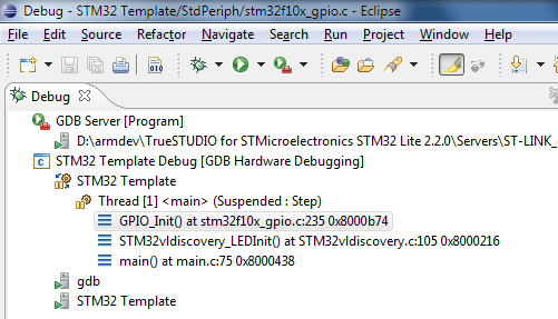
The built-in ST-Link on the ST Discovery board also supports live debugging of the program running on the Cortex M3. If you’re coming from the Arduino, or vanilla AVR development with an AVRISP mkII programmer that lacks debugging capability, this is a quantum leap forward. The people who wrote the Eclipse + Code Sourcery + STM32 setup guide also wrote an excellent hardware debugging setup guide, so I won’t repeat the steps here. Unfortunately, it involves downloading the entire Atollic Lite toolchain (250MB) just to get the ST-Link compatible gdbserver it contains. This also requires registering with Atollic, and getting a (free) activation key. It’s a hassle, but you only need to do it once.
Debugging works just how you’d expect. You can step through running code, set breakpoints, examine variable values, and view the call stack. Stepping through code seems unexpectedly slow, taking 1-2 seconds to step over a single line. The gdbserver also crashed a few times while I was debugging, and the only clue was that attempts to start a new debugging session failed with a generic error. I also found that stepping over a line that branches to itself, like
for(; nCount != 0; nCount--);
put the debugger into a state where the program was suspended, but the debugger thought it was running, forcing me to press the “pause” button to regain control. The overall debugging experience was a bit rough around the edges, but was much better than nothing. A different toolchain might have provided a smoother debugging experience, and I don’t fault the Cortex M3 or the ST Discovery board hardware for the debugging problems I encountered.
Beyond the Examples

Running through the examples is a good way to get familiar with the Cortex M3, but to really learn what it’s like to develop for, there’s nothing better than creating your own custom project. Using the LED blink program as a template, I was able to port some code for controlling a Nokia 5110 LCD display, and print the message shown in the photo. The LEDs, transistor, and resistor in the upper right are from an unrelated circuit on my breadboard, and the only connections between the Discovery board and the LCD are the seven wires at the bottom.
My example program shows the code used to print the message on the LCD. There were no real surprises during development, and it only took me about 30 minutes to get the LCD working with the ST Discovery board. The only oddity I encountered was that there doesn’t appear to be a calibrated wait/delay function anywhere in the STM32 libraries. I wrote my own delay_ms() function that’s roughly accurate, assuming a 24 MHz clock and code compiled in the Debug configuration. It’s an imperfect solution, so if there’s not already a suitable delay function somewhere in another ARM library, it will probably be necessary to use a timer to get delays independent of clock speed and compiler options.
The GPIO_ library is great for getting projects up and running quickly. For high-speed performance-sensitive designs, however, there may be an unacceptable amount of overhead involved in calling a library function every time an I/O pin needs to be manipulated. In practice, the compiler may inline these functions when building Release configuration code, but I didn’t investigate to confirm it.
When powered by USB, the voltage at the ST Discovery board’s 3V3 pin is only about 2.97V, with no load. That might cause problems for some devices, but the Nokia 5110 LCD worked fine at that voltage.
Conclusions

Are the Cortex M3 and STM32 Discovery board what you’ve been looking for? In what kinds of projects do they fit best?
As an alternative to an Arduino or vanilla AVR board, the STM32 Discovery board looks like a clear winner in terms of price and hardware. It has more I/Os, more peripherals, larger memories, faster core clock MHz speed, and more performance per MHz due to its 32-bit internal design. All that, and it’s priced at less than half the cost of an Arduino.
What the STM32 Discovery lacks is easy-to-use development tools, and a large community of other users to collaborate with. The method I used to create a toolchain is probably too complex for many beginners, and they won’t be able to afford the commercial alternatives, so they’ll likely be shut out of Cortex M3 development entirely. Even if they do get the toolchain installed successfully, they won’t find the wealth of examples, 3rd-party libraries, or other support materials that exist in the AVR world. The value of that support shouldn’t be underestimated. Performance and memory aren’t everything.
The STM32 Discovery board is better matched for experienced microcontroller developers who’ve already done some work outside the Arduino environment, and are ready to accept additional complexity in exchange for major hardware improvements. The 24 MHz 32-bit Cortex M3 on the STM32 Discovery board is already a nice step up from 8-bit AVRs, but it’s just the beginning of the Cortex M3 line. Higher-end members of the Cortex M3 family can perform complex real-time tasks not possible on an AVR, drive high resolution color displays, run a real-time micro-OS capable of scheduling many programs at once, or even run Linux. For those who need this kind of power, the Cortex M3 is a great choice.
Read 10 comments and join the conversationXilinx vs. Altera Tools For Hobbyists
I used to believe that Altera’s FPGA tools were much more hobbyist-friendly than the comparable Xilinx tools, and I frequently bashed the Xilinx tools whenever the topic came up. But after giving them a head-to-head comparison recently, I think I may have to eat my words. The truth is they’re both pretty rough and clunky, and difficult for a beginner to get the hang of, but the Xilinx tools are definitely superior in some important areas.
My FPGA apprenticeship started out poorly with Xilinx in 2009. Over the couple of years I’ve owned a Xilinx Spartan 3A FPGA starter kit, I’ve learned to really hate it and the confusing Xilinx tools and documentation. Trying to get the DDR2 DRAM working on the Xilinx board was an exercise in futility that occupied several months of my time, and I eventually just gave up, as I couldn’t even get the reference design to work. The Spartan 3A starter kit hardware also seems needlessly complex, like they threw one of every possible component on there just to serve as an example. That makes it a confusing mass of jumpers, options, and shared pins that obscures whatever you’re trying to create. Too often I also found the Xilinx documentation and examples incomprehensible, and their online support poor to none. Eventually I gave up on them, and vowed to only use parts from their competitor Altera in the future.
A year or so later, the opportunity to try Altera hardware and tools came, during the development of Tiny CPU. It was a mostly positive experience, although I didn’t really attempt anything very complex. When I needed it, I found the Altera documentation to be decent, and the project went forward without ever hitting any Altera-specific snags. I viewed the result as promising, but not really conclusively better than Xilinx.
During the recent development of Plus Too, I’ve finally had an opportunity to try both Xilinx and Altera tools for the same project, and make a direct comparison. I first spent about a week gettings things set up on the Xilinx board, which culminated in the “Sad Mac” I wrote about yesterday. Then for the past two days, I’ve been translating the existing design to get it working on the Altera board. I love the Altera DE1 hardware– it’s uncluttered, has SRAM *and* SDRAM, and comes with a nice program that can be used to interactively control the hardware or read/write the on-board memory. When it comes to the tools, however, moving from Xilinx to Altera definitely felt like taking a step backward.
Windows 3.1 called. It wants its interface back.
My first complaint about the Altera tools is the interface, which is a UI gem straight out of 1993. Yes I know it’s a petty complaint, but it reinforces the feeling of cruftiness that permeates everything else in the Altera tools. Check out a couple of screen shots:


Those message tabs remind me of MSVC 6.0. And the navbar icons use about nine unique colors across the whole set. And what’s with the balloon help menu?
Here are the corresponding sections of the Xilinx interface for comparison:


That feature is not licensed and has been disabled
Another gripe about the Altera tools is that so many features have been locked out of the free edition. I understand they need to hold something back for the professional edition of their tool, but some of the things they lock just seem petty. After a full compilation run, the output window will be full of warnings about all these tantalizing features you’re not getting. For example if you synthesize your Altera model on a computer with a multi-core CPU (pretty much any CPU these days), you’ll get this warning:
WARNING: Parallel compilation is not licensed and has been disabled
Thanks for nothing, Altera. The Xilinx tools happily spins off multiple threads for each of my CPU cores, and tells me it’s doing it too.
What simulation?
An essential part of FPGA development is simulating the design, because it’s generally much easier to find mistakes in simulation than in the real hardware. You can view every waveform, step through time, set breakpoints, and other sorts of things like you’d do in a functional programming language like C. With the Xilinx tools, I was able to simulate the Plus Too design by switching to the Simulation view, and double-clicking Simulate Behavioral Model. The built-in simulation tool ISim started right up, and within moments I was debugging the design, watching the simulated CPU talk to simulated RAM, ROM, and video. Professionals might need something more powerful than ISim, but it was great for my needs.
The Altera simulation experience was a nightmare in comparison. It took me some time to realize that the Altera Quartus II software doesn’t include any built-in simulator, so I wasted quite a while assuming I was doing something wrong when simulation didn’t work. Altera recommends that you use Modelsim Altera Edition, which is a separate product that must be downloaded and installed separately. Once that’s done, you need to go back into the Altera software and tell it to use Modelsim as the simulation tool, which involved more poking around in menus that are doubtless familiar to pros but took me a while to discover.
Once I had Modelsim AE launching with my design, I thought I was home free. Instead, I was greeted by a laundry list of errors like “Unresolved defparam reference to ‘altpll_component’ in altpll_component.port_extclk3.” After some more swearing and poking around, I found that Modelsim was relying on some environment variables that weren’t set. Environment variables… OK. I made the necessary environment settings, but it still didn’t work. It seemed that Modelsim was unable to parse the definitions for any Altera megafunctions (their IP blocks). A few hours of Googling for answers didn’t find any obvious solutions. It seemed that it might somehow be related to instantiating megafunctions with VHDL implementations from inside a Verilog file, but all my megafunctions were created by the Altera wizard, so they should be fine right? Wrong. Eventually I hand-edited the modelsim.ini file to force it to use Verilog implementations of the megafunctions instead of VHDL ones, and that worked. There was probably some simpler way to do it, but I never found it.
You got your VHDL in my Verilog
Once the simulation model finally compiled successfully, I was ready to start debugging, only to be met with the error message “ALTERA version supports only a single HDL”. Huh? The translation is “you can’t simulate designs containing both Verilog and VHDL files unless you buy the commercial version of ModelSim for over a thousand dollars”. Since my design files are Verilog, but the TG68 68000 core is VHDL, that meant I was dead in the water. In contrast, Xilinx’s ISim simulated all this with ease and no complaints.
It’s the software, stupid
For most of us electronics hobbyists who are interested in FPGAs, the choice of what device or board to use isn’t really determined by which has the most 18-bit multipliers or other whiz-bang features. It’s not really determined by the cost, either, since generally we’re only buying one device. Instead, it’s determined by how easy the device is to use, and how quickly we can accomplish our goals with the hardware. The best software tools are like a trusty set of wrenches that let us quickly open things up and tinker with them, focuing our attention on the novel parts of the project. Poor tools force you to spend time thinking about them instead of your project, and I wish there were better FPGA tools options for hobbyists. From the two major FPGA vendors, my nod goes to the Xilinx tools if you care strongly about simulation.
Read 20 comments and join the conversation
Understanding Verilog Warnings
Those of you who’ve followed the blog for a while know about my many frustrations with Verilog. Because it feels sort of a like a procedural programming language, but very definitely isn’t one, I keep expecting to be far more competent at Verilog design than I actually am. While working on Plus Too, the Xilinx synthesis tool reported many, many warnings that I didn’t understand. The warning list grew to at least 100, and was so long that I just stopped reading it. That was dangerous, as most of the warnings were likely problems that needed to be addressed.
I’ve been writing C and C++ programs for years, and I’m very comfortable with the language, its details, and the compiler warnings and errors produced by various mistakes. I normally find the warnings easy to understand, because they reference a specific file and line number, and use well-known terminology to describe the problem. Sure, some more obscure errors like “not an lvalue” would probably flummox a beginner, but at least he’d know what line to scrutinize.
Most Verilog warnings I see are non-localized, and do not reference a specific file or line number. They are design-wide warnings, resulting from an analysis of all the modules in all the .v files. This can make it unclear where to even being looking for the cause of a warning. A typical example is something like:
Xst:647 – Input <vblank> is never used. This port will be preserved and left unconnected if it belongs to a top-level block or it belongs to a sub-block and the hierarchy of this sub-block is preserved.
OK, there’s an unused input named vblank. But where? The vblank signal is routed through half a dozen different modules in the design, so how do I know which one I messed up? The only solution I’ve found is to search the whole project for all references to vblank, and verify each one. I also find that error message much too wordy.
Another example:
Xst:646 – Signal <ramAddr<0>> is assigned but never used. This unconnected signal will be trimmed during the optimization process.
This is basically the same as the first example, but has a totally different warning message. Why? Because one is single combinatorial output, and one is a bit in a register? Then there’s this:
Xst:2677 – Node <ac0/vt/videoAddr_17> of sequential type is unconnected in block <plusToo_top>
It’s essentially the same issue again, but yet another totally different warning message. This time it gives the name of the offending module, so it should be easier to track down.
The general meaning of all these warnings is fairly clear: some expected signal connections are missing. Find the problem, and either add the missing connection, or suppress the warning if the unconnected signal is intentional. There were two other warnings I saw frequently whose meanings were definitely not clear to me, however:
Xst:2042 – Unit dataController_top: 34 internal tristates are replaced by logic (pull-up yes): cpuData<0>, cpuData<10>, cpuData<11>, cpuData<12>, cpuData<13>, cpuData<14>, cpuData<15>, cpuData<1>, cpuData<2>, cpuData<3>, cpuData<4>, cpuData<5>, cpuData<6>, cpuData<7>, cpuData<8>, cpuData<9>, mouseClk, mouseData, ramData<0>, ramData<10>, ramData<11>, ramData<12>, ramData<13>, ramData<14>, ramData<15>, ramData<1>, ramData<2>, ramData<3>, ramData<4>, ramData<5>, ramData<6>, ramData<7>, ramData<8>, ramData<9>.
Um, what? This meant nothing to me. I wasn’t even sure if replacing internal tristates with logic was good or bad. The Xilinx tool shows each warning as a link you can click to get more info, but sadly it doesn’t work. Clicking the link just opens a web browser and does a search on the Xilinx site for “Xst:2042”, which returns no results. In fact, none of the synthesis warning links work. If a warning doesn’t make sense to you, you’re on your own.
After a lot of searching around on other web sites, I finally found a decent explanation. It seems that some (or all?) Xilinx devices do not support tristate logic (a signal with an output enable) anywhere but on the actual I/O pins. Signals internal to the FPGA can not be tristate. Tristate logic is typically used to enable multiple drivers to operate on a single shared bus, one at a time. So instead of using internal tristates, you need to construct your design using additional logic to select which module’s data should appear on the shared internal bus, using a mux or similar method.
That mostly makes sense, but I’m using the FPGA to simulate a system of separate parts (address controller, data controller, CPU, RAM, etc) that will eventually be physically separate chips communicating with tristate logic on shared busses. I don’t want to rewrite my design to eliminate tristate logic, because tristate logic is what will be used for these chips. For now I’ve left the logic as is, and I’m ignoring the warnings, and it seems to be working OK. I’m unclear exactly what the synthesis tool has substituted for the internal tristates, though– “logic (pull-up yes)”? What is that, and what problems might it cause?
The other confusing warning that’s been plaguing the design is:
Xst:2170 – Unit plusToo_top : the following signal(s) form a combinatorial loop: ramData<0>, ramData<0>LogicTrst20.
Xst:2170 – Unit plusToo_top : the following signal(s) form a combinatorial loop: ramData<1>, ramData<1>LogicTrst20.
…
…and so on, for every bit of ramData. This stems from my attempt to specify a bidirectional bus driver akin to a 74LS245:
assign ramData = (dataBusDriverEnable == 1’b1 && cpuRWn == 1’b0) ? cpuData : 16’hZZZZ;
assign cpuData = (dataBusDriverEnable == 1’b1 && cpuRWn == 1’b1) ? ramData : 16’hZZZZ;
This driver has ramData on one side, and cpuData on the other. When it’s enabled, it drives data from one side to the other. The direction in which data is driven is determined by the cpu read/write line. So why does this form a combinatorial loop? I’d expect to see that warning for something like:
assign a = b & c;
assign b = a & d;
but my bus driver code looks OK to me. I still haven’t found an explanation for this one, but I think it’s related to the previous issue about internal tristates. The synthesis tool is probably replacing my bidirectional bus driver tristates with some other logic, which then forms a combinatorial loop. I’m not sure how to fix this one without rewriting the design to use a different method than tristates. But again the final project will see ramData and cpuData on I/O pins connected to other chips using tristates, so I don’t want to rewrite the design.
Read 7 comments and join the conversation
JTAG, EXTEST, and hair loss
 Oof. See that window to the left? That’s the result of 10 hours of debugging effort on bring-up for my custom Tiny CPU board. What you see is UrJTAG connected to the JTAG interface of the Max II CPLD, and successfully detecting the 29LV040B flash ROM that’s also on the board. Getting to this point was a long process covering everything from software to cleaning up bad solder joints.
The good news: I’ve soldered the Max II CPLD, Flash ROM, and SRAM to the board, and they seem to be working. By using UrJTAG and the EXTEST instruction, it’s possible to disconnect the CPLD’s core logic from the pins, and set the pin states to any arbitrary values. The software also needs to be told which pins are connected to the address bus, data bus, CS, OE, and WE. Once that’s done, it’s possible to read and write any non-JTAG device whose pins are connected to the CPLD, by bit-twiddling the CPLD pins. Using UrJTAG’s commands for memory access, I’ve successfully written and read from the on-board SRAM, and reprogrammed the on-board Flash ROM. That should be nearly everything that’s needed to start work on the Tiny CPU core itself.
Interaction with the Programmed Design
I find JTAG and especially the UrJTAG tool to be maddeningly difficult to understand. Things don’t work how I’d expect, or don’t work at all, and I can’t be certain if it’s a hardware problem, software bug, or misunderstanding on my part. The best example is the reason that it took me so long to reach the point where the Flash ROM was successfully detected: interaction between the core logic (the design programmed into the CPLD) and the EXTEST pin manipulation. From what I’ve read, there should be no interaction. When the EXTEST instruction is executed by the JTAG controller, then the pins should be decoupled from the core logic. It shouldn’t matter at all what design is programmed into the CPLD, what that design wants to do with the pins, or whether any design is programmed at all.
After long experimentation and electrical testing, I discovered that the core logic design does matter when interfacing to other devices with EXTEST. Whether this is normal, or the result of a boundary scan software bug in UrJTAG, I don’t know. What I found is that if I programmed the CPLD with a design that declared the data bus as type inout (which it is, of course), then I could read from the SRAM and Flash but not write to them. By sticking a multimeter on the pins, I found that data bus pins driven to a logical 0 using EXTEST worked fine, but data bus pins driven to a logical 1 just went into a high-Z state instead, so I could never write a ‘1’ bit. I also learned that if I set the data bus type as output, then I could no longer read from the RAM or Flash. Only when I set the data bus type to input could I both read and write using EXTEST. This is nonsense on a several levels, as it shouldn’t be necessary to reprogram the CPLD with a new design just to use the EXTEST functionality. The only explanation I can think of is that the boundary scan register uses 3 bits to define the state of each pin (input, input with pull-up, output driving 0, output driving 1, output driving Z, and a few others) which UrJTAG may not handle properly, with some bits carrying over from the programmed design. I had a similar problem when using a trial version of TopJTAG Flash Programmer, however, so I’m not sure I can blame the software.
JTAG Bit-Banging
As another example of UrJTAG strangeness, the board has an LED connected to IO97, such that the LED illuminates when the pin value is 0. It should be possible to blink the LED using UrJTAG’s set signal command, e.g:
jtag> set signal IO97 out 0
After much tearing out of my hair, I learned that while that’s part of it, it’s also necessary to explicitly put the device in EXTEST instruction mode first, and explicitly shift the instruction and data into the device, as UrJTAG does none of this for you:
jtag> instruction EXTEST
jtag> shift ir
jtag> set signal IO97 out 0
jtag> shift dr   (the LED turns on)
A little cumbersome, but at least it works. In contrast, I was never able to get the corresponding get signal command to work at all. After setting IO97 to 0 as above, which visibly turns on the LED, the value of IO97 still reads as 1:
jtag> get signal IO97
IO97 = 1
jtag> shift dr
jtag> get signal IO97
IO97 = 1
The ability to twiddle pins arbitrarily through JTAG could be a huge aid to debugging, but not if the corresponding ability to read the current pin state doesn’t work.
If anyone has some experience using UrJTAG for this kind of troubleshooting, please leave a comment, or contact me by email. Thanks!
Read 5 comments and join the conversationEagle vs. KiCad
 I spent a little time evaluating Eagle and KiCad, two well-regarded pcb design tools for hobbyists, to see which one would best meet my needs for Tiny CPU’s board design. As a complete beginner who’s never made any kind of circuit board before, my priorities are doubtless different from what other people may value, but hopefully this comparison will be useful for others in a similar situation. My testing methodology was to follow Sparkfun’s Eagle tutorial, which involves creating a simple board based around an FTDI USB chip, and then to repeat the same tutorial creating the same board using KiCad.
The short version of my conclusions is that both packages work nicely, and will get the job done. For most people, though, I believe Eagle will be the better choice.
Eagle
I used the free version of Cadsoft Eagle, which has all the features of the commercial versions, but limits you to a single schematic page, 2 layers, and a 10 x 8 cm board area. For this test, I used Eagle 5.8.0.
The Good
Eagle’s biggest strength is its near universal adoption. Sparkfun has a huge library of Eagle parts and footprints, and their tutorials use it as well. Ladyada’s site also has an Eagle library. Most pcb manufacturers will accept Eagle .brd files directly, enabling you to skip the Gerber output step completely. There’s also a tremendous amount of information available online about how to use Eagle, answers to common and not-so-common questions, tutorials, and other data. Choosing Eagle puts you in the mainstream as far as hobbyist pcb design goes, for better or worse.
I found Eagle fairly easy to use for a complete beginner. I was able to go through the FTDI tutorial from start to finish in about an hour. The software felt reasonably logically designed, and I didn’t have to guess too much how to do things. Going from the schematic to the pcb layout was pretty straightforward. The auto-router worked fairly well and routed the entire board. Afterward, I went back and ripped up some tracks, relaying them by hand to see how that experience was. The pcb layout tool automatically showed the 10 x 8 cm board outline, which I resized to make a smaller board. The design rule checker stepped through potential issues one at a time, highlighting each one nicely.
The Bad
Depending on your project, the 2 layer and 10 x 8 cm limits may be a problem. If you need more, you’ll have to buy one of the commercial versions, which will set you back between $500 and $1500, out of the reach of most hobbyists. Or you’ll have to split you design into multiple boards.
Cost aside, I do have a few other gripes. The default keys for actions like move, copy, delete, and place wire are all function keys instead of letters with some relationship to the actions. I found that made it a bit of a challenge to remember what F4 does, but I assume the settings can be changed, so it’s not a big deal.
Identifying the right components by footprint was a bit of a pain. When you go to place a new component, it shows a preview of the footprint, but there’s no sizing grid or other dimension information. That made it impossible to tell if I was selecting a capacitor footprint with the leads 1 mm apart, or 1 inch.
My biggest gripe was with the pcb layout tool: not enough things are labeled on your board as you lay it out. I looked for some options to change this, but didn’t find any. Once you place a few parts, route some traces, and get everything nice, the board starts to look like a random sea of red, orange, and white geometric shapes. Pin numbers and net names are not shown. You can click on a pin or net, and it shows the name in the status line, but that’s a bit cumbersome.
Final Cut
Overall I liked Eagle a lot. It definitely feels as though it’s stood the test of time, and would be able to meet just about any challenge I could think of. My only real complaints are the limitations of the free version, and the visual confusion with a busy pcb layout.
KiCad
KiCad is an open-source software tool for pcb design. It often gets mentioned as a better, free alternative to Eagle, and I’ve heard a few people say that if it had been around earlier, it would have become the de-facto standard for hobbyists instead of Eagle. For this test, I used KiCad build 20100406.
The Good
I was surprised at how polished KiCad feels. It definitely surpassed my expectations for an open-source tool. In fact, its interface is more attractive than Eagle’s, and is arguably a bit more intuitive too. Actions are bound to letter keys (move is M for example), which speeds learning.
The pcb view in KiCad is pretty nicely done, with everything well-labeled. If you zoom in far enough, individual tracks are even labeled along their length, like streets on a map. This made my layout and routing job easier.
When selecting a footprint, the preview shows it on a 0.1 inch grid, which was a big help in identifying the right ones.
KiCad is open source, which is a good thing in my view. It’s free, of course, with no limits on number of layers or board size. And the source code is freely-available too, so if there’s a behavior you don’t like or a feature you really want, you can always grab the code and do it yourself.
The Bad
I have just one major complaint with KiCad, and that’s the method of footprint selection. With Eagle (and most other similar tools), a “part” combines a logical description for the schematic view and a physical description for the pcb view. When I choose FT232RL from the library in Eagle, it not only knows that it has pins named things like TX and RX, but it also knows that it’s a 28-pin TSSOP package. After I finish my beautiful schematic, I can go straight to the board, and start laying out the chips.
In contrast, KiCad divorces a part’s logical description from its physical one. When I choose FT232RL from the library, it knows it has TX and RX pins, but when I finish the schematic I have to go through a footprint-assignment step before I can start laying out the pcb. I get a window that says FT232RL on one side, and a giant scrolling list of 418 possible footprints on the right side. Sorry, but that stinks. I use parts from a library so that I don’t have to go sifting through a million data sheets for that kind of info. And if I spend three weeks building a huge schematic for my electronics masterpiece, when I get to the footprint assignment step, am I really going to remember whether JP45 was supposed to be a Molex or a DIN connector? Separating logic from footprint probably makes sense in an abstract sense, but in practice, the workflow stinks.
The rest of KiCad was mostly great, but marred by several little annoyances. I found that the screen would predictably get “droppies” whenever I edited a wire in the schematic view, or updated the rat’s nest in pcb view, so I was constantly pressing F3 to refresh the window.
The quality of the few parts and footprints I examined seemed poorer than Eagle’s. The USB-B footprint did not indicate the correct edge. The FT232RL schematic did not have hidden power pins marked as hidden correctly. When choosing footprints from the giant list of 418, many of them were acronyms for something in French.
Moving or rotating a component on the schematic view broke the wires connected to it, instead of moving or rotating the connections with it.
The rat’s nest in the pcb tool seemed to have a few drawing problems. Only the rat’s nest wires for components nearby the one being moved were drawn, instead of all of them. Where there was a choice about what other parts and pins to draw lines to, KiCad’s rat’s nest renderer seemed to make poorer choices than Eagle’s, resulting in a more confusing depiction of the nets.
The board outline was not added automatically. It took some investigation to find and view the PCB Edges layer, and draw a rectangle shape into it to indicate the board. I couldn’t figure out how to add mounting holes at the corners of the board, as I did with Eagle.
The KiCad auto-router didn’t appear to work reliably. When invoked, it routed just one net, leaving the rest as air wires. I tried routing a few more nets myself and then auto-routing the rest, but I was never able to make it do anything at all after that first net.
The software seemed to become confused when I crossed two ground routes without actually making a node to join them explicitly. It permitted me to cross them without complaint, which it wouldn’t otherwise do for unrelated routes. But it behaved as if the two routes were unconnected, telling me that some pins still needed connections to ground when in fact they already were connected.
The KiCad design rule check seemed a bit awkward. All the DRC violations were highlighted at once in the pcb view window. When I clicked on a single violation in the list to highlight the corresponding item in the pcb view, it popped up a disambiguation window instead. I think this was because it was trying to reference a specific x,y position in the view, which was overlapped by several elements. The DRC also flagged the entire SSOP28 footprint as a violation, complaining that every pad was too close to its neighbors.
Final Cut
Despite these many little problems, KiCad is quite a polished and powerful product. For someone who’s built a few circuit boards before, has their own component library, and generally knows more-or-less what they’re doing, the little annoyances should be easy to work around. The lack of layer or size restrictions and ability to add new features are big pluses. Complete beginners will probably get thrown off by some of the software’s quirks, however, and may only want to consider KiCad if the layer and size limits of Eagle’s free version are an issue.
Read 43 comments and join the conversation