

Archive for the 'BMOW 1' Category
Schematics!
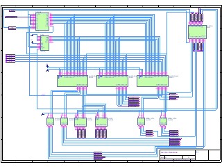 The first draft of the BMOW schematics are finished, along with complete equation lists for the 11 unique GALs (18 GALs total). This is everything needed to actually build the machine. You can view it all on the technical info page, along with an updated block diagram.
Whew, what a job that was! The datasheets, the timing diagrams, the insomnia… I’m really beginning to question my own sanity. If some of the schematics seem a little confusing and convoluted, it’s probably because I was asleep while I drew them. Ditto for the spaghetti wire paths.
I’m going to step back now and review the whole system, looking for any blunders I’ve made, or any opportunities for improvement. I hope that the people who’ve been following my progress can find some time to review the plans as well. Your design feedback is welcome and appreciated!
Initial Schematics Complete
The first draft of the schematics are complete. It was a good exercise, as working out every connection for every chip forced me to consider a few points I’d glossed over before. I ended up having to introduce a few more components than I originally planned on, to help generate needed control signals, or work around timing problems.
The memory and device schematics were the most difficult. As I wrote about previously, the timing requirements for the memory and USB module required careful design in order to avoid constraining the clock speed too severely.
The LCD module proved even more troublesome. It has some truly horrible timing constraints, including an 80ns setup time for data, and a minimum 230ns pulse width for the write enable signal. I couldn’t find a way to connect it directly to the memory data bus without slowing the clock down to below 2MHz. Instead, data for the LCD is actually written to a special register, and then on the next clock cycle, dedicated control logic writes the register value to the LCD. During cycles where the LCD isn’t being written, I’ve configured things so that it will always read the LCD busy flag. That means it’s impossible to read any other data from the LCD, like what character is currently at each location on the screen, but I can’t imagine why you’d want to do that anyway.
Now I need to go back through all the schematics, clean them up a bit, and check for places where I’ve exceeded TTL fanout limits (generally each output can feed no more than 10 inputs). Then I need to write the equations for all the GALs called for in the schematics: 18 in all. Once everything’s ready, I’ll post it up here for feedback.
Be the first to comment!More Timing Analysis
The schematics are nearly done. I’ve finished all of them except the memory/device subsystem, which is proving to be difficult. Unlike the registers and all the other machine components, the RAM and the USB interface don’t use a clock. Instead, they have a write-enable signal that causes data to be written the instant the signal is asserted. That means I need to take extra care to prevent the write-enable signal from being momentarily asserted while the state of the machine is changing from one instruction to the next– something that’s not necessary for clocked components.
The common strategy I’ve seen is to combine these kinds of write-enable signals with another signal that’s guaranteed to be asserted only when the write-enable signal is sure to be valid. Typically, this is the clock signal itself, or something derived from the clock signal. For example, if the write-enable signal is active low, it can be OR-ed with the clock signal, and the result will only be low if write-enable is asserted and it’s the second (low) half of the clock cycle. This allows the write-enable signal to temporarily take on invalid values during the first half of the clock cycle without harm.
I did a static timing analysis, based on my schematics and the chip datasheets, and in the worst case it will be 233ns from the start of a clock cycle until the write-enable signal and memory address are guaranteed valid. If I use the clock signal to combine with the write-enable signal, then the clock period must be at least twice 233ns, so 466ns, or 2.14MHz. I’d like to go faster than that.
My clock module also generates a signal called Q1, that lags the main clock (Q0) by a quarter cycle. By OR-ing together Q0, Q1, and write-enable, the result will only be low if write-enable is asserted and it’s last quarter of the clock cycle. That implies a limit of 233ns for three-quarters of the clock cycle, so 310ns for the whole cycle, or 3.22MHz. That’s a little better.
Unfortunately, using Q1 and Q0 to mask write-enable until the last quarter-cycle causes problems with the USB inteface. The USBMOD4 needs to have its read-enable input gated as well, because reading actually changes the state of the device by advancing its internal FIFO. Once read-enable is asserted, it can take up to 50ns for the USBMOD4 to put valid data on the output pins. Data must then pass through the 74LS245 bus driver (40ns), and arrive at the destination register 20ns before the end of the clock cycle to observe the setup time requirements. Therefore the quarter cycle must be at least 50 + 40 + 20 = 110ns, so 440ns for the whole cycle, or 2.27MHz. That’s hardly any better than the 2.14MHz achieved by using Q0 alone and ignoring Q1.
So for two different reasons, it appears that the machine will be limited to a top speed of 2MHz. With some redesigning, I could probably speed that up, but I’m more interested in just getting it working right now than in getting the fastest possible performance. It’s entirely likely that in practice I’ll be able to run faster than 2MHz, since all of my numbers are the worst-case figures from the datasheets. The listed “typical” numbers are generally about 1.5x faster than worst-case, so it might be possible to run as fast as 3MHz with the current design.
For the curious, the time-limiting path from beginning of a clock cycle to valid read/write-enable and memory address is:
| Cumulative Time | Delta Time | Path |
|---|---|---|
| 0 | 0 | clock cycle begins |
| 35 | 35 | 74LS194 condition code register’s new values are valid, and used as micro-ROM inputs |
| 105 | 70 | 29F010 micro-ROM output |
| 143 | 38 | 74LS139 decodes address register enable from micro-ROM output |
| 168 | 25 | 22V10-based address register’s output is ready |
| 193 | 25 | 22V10 address decoder determines if address is in program ROM, RAM, or memory-mapped hardware |
| 233 | 40 | 74LS138 decodes read/write-enable signals for specific hardware devices |
Follow up: After a more careful reading of the datasheets, things aren’t quite as bad as I’d first thought when combining Q1 and Q0 to mask the enable signals to the last quarter clock cycle. First, the worst-case data propagation delay for the 74LS245 is only 12ns, not 40. The 40ns figure is for the output-enable signal on the ‘245, which should already be set by the time the data is coming through. Second, the setup time at the data registers is actually 15ns, not 20. Add up the 50ns delay from the USBMOD4, 12ns at the ‘245 bus driver, and 15ns setup time, and you get 77ns. Coincidentally, that’s precisely the amount of time allowed by a 233ns time for three-quarters of the clock. So the limitation imposed to guarantee valid read-write/enable signals exactly matches the limitation imposed to guarantee valid data read from the USBMOD4, at a clock period of 310ns for the whole cycle, or 3.22MHz.
Be the first to comment!Piles of Hardware
I keep accumulating more and more hardware, and my office is beginning to overflow with boxes, tools, and wires. I need to start turning this pile of parts into an actual machine ASAP.
The first of my recent acquisitions was a replacement universal programmer, an EasyPro 90B to replace the TOP 2007 that had problems programming GALs. Yes, I’m replacing one no-name programmer from China with another, but in this case the EasyPro 90B seems to work fine. If I’d read reviews before making my original purchase, I could have saved myself a lot of hassle. The whole TOP line has received universally poor reviews, from what I’ve seen. Both the EasyPro and the TOP programmers were ordered from www.mcumall.com, who offered to exchange the TOP programmer after I wrote about my problems in their online forums.
My second new hardware arrival was a USBMOD4 interface module, for connecting my computer to a PC via USB. It couldn’t be simpler to use. Install the driver, and it appears as an additional COM port on the PC. Connect a USB cable to the USBMOD4, launch a terminal program, and every keypress is transmitted and stored in the USBMOD4’s FIFO buffer. An output pin changes state when the FIFO has data in it, which the computer can sense and then enable the USBMOD4 to drive the next FIFO byte onto the data bus. I was able to put together a test circuit to read data from the PC using a protoboard in about 30 minutes.
The only problem I have with the USBMOD4 is that it appears to be hardwired to draw its power from the USB cable, rather than from the system’s power supply. This means that it’s “on” as soon as the USB cable is connected, regardless of whether BMOW is turned on or off. What’s worse, if I connect the USBMOD4’s power pin to BMOW’s power bus, BMOW will turn on as soon as the USB cable is connected. I need to isolate the USBMOD4’s power from the rest of the machine’s, while still allowing for data to be passed between them. This may be a little complicated. I’m assuming it’s OK to connect their grounds, even though theoretically the PC’s ground might not be at the same electrical potential as BMOW’s. The bigger problem is that the active low signal from the USBMOD4 that signals when there’s data in the FIFO will be low if no USB cable is connected, because there will be no power to it. This will make BMOW think there’s data to be read. I think I can solve this by using a pull-up resistor connected to BMOW’s +5 supply. If anyone’s ever done something similar before, I’d love to hear about it.
I also bought an HP 1631D logic analyzer off eBay, although it hasn’t arrived yet, and it was an extra cheap ($35) unit in as-is condition. It’s a combination 100MHz bandwidth digital oscilloscope and 48 channel logic analyzer. A logic analyzer records a history of the logical value (0 or 1) of a set of signals, like an address bus or data bus. It can be used to help debug hardware problems, like why a computer locks up when it reaches a certain address. Basically, it’s a hardware debugger.
I’m sure there was a point in my life (like 2 months ago) where I assumed anyone who had a personal oscilloscope in their home was the biggest nerd imaginable.
Read 4 comments and join the conversationDas ist kein 6502
I received an email from CPU-builder Dieter Müller, describing his very impressive M02 project to build a custom CPU binary compatible with the 6502, using standard 74LS and similar parts. In short, a project quite similar to my own, except that he’s already done it. Take a look at the photos and hardware description on his site http://freenet-homepage.de/dieter.02/m02.htm. He even got the Commodore 64 kernel and BASIC running on the M02.
Read 1 comment and join the conversationSchematics
I’ve started creating schematics for the machine, using an evaluation version of CSiEDA 5. Making a real schematic that shows all the parts, pins, and interconnections is amazingly time-consuming, but it’s essential if I want to avoid making construction mistakes.
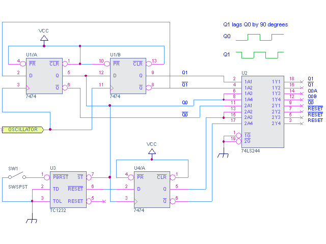
It took me a couple of hours to get familiar with CSiEDA and create this schematic for the clock and reset generation circuitry. A crystal oscillator is used to clock a pair of flip-flops, wired so as to produce two new clock signals, Q0 and Q1, at a quarter the frequency of the oscillator input. Q0 is the primary clock signal, and is used by most other clocked components in the system. Q1 lags Q0 by 90 degrees (one-quarter of a cycle), which is useful for generating other timing signals. The clock signals are buffered by a 74LS244, which has a higher drive current than most TTL chips, meaning each output pin can drive up to 16 other TTL inputs. Some signals appear on multiple ‘244 output pins, where I expect to need them at more than 16 inputs elsewhere in the system.
A Microchip TC1232 supervisor chip is used to generate the /RESET signal. Whenever the +5V input to the TC1232 is too low (during power-on, power-off, or power glitches), it forces the /RESET signal active for about 100ms, restoring the machine to its initial state. It also has an input for a reset switch, with built-in pull-up resistor and debouncing circuitry. The /RESET signal is clocked through another flip-flop, so the rest of the system will only see /RESET change at a clock edge, rather than in the middle of a clock cycle.The TC1232 also has a “watchdog” feature that can be used to auto-reset the machine if it crashes. The CPU is expected to toggle the TC1232’s strobe (/ST) input periodically to indicate that it’s still alive. If too much time passes without /ST being toggled, the TC1232 will force the /RESET signal active. I don’t plan to use this feature, so I’ve tied /ST directly to the clock signal, so it will always be toggling.In the final implementation, the flip-flops and 74LS244 may all be replaced by a single GAL, but the functionality will remain the same.
Read 2 comments and join the conversation