

Archive for the 'BMOW 1' Category
First Bootup!
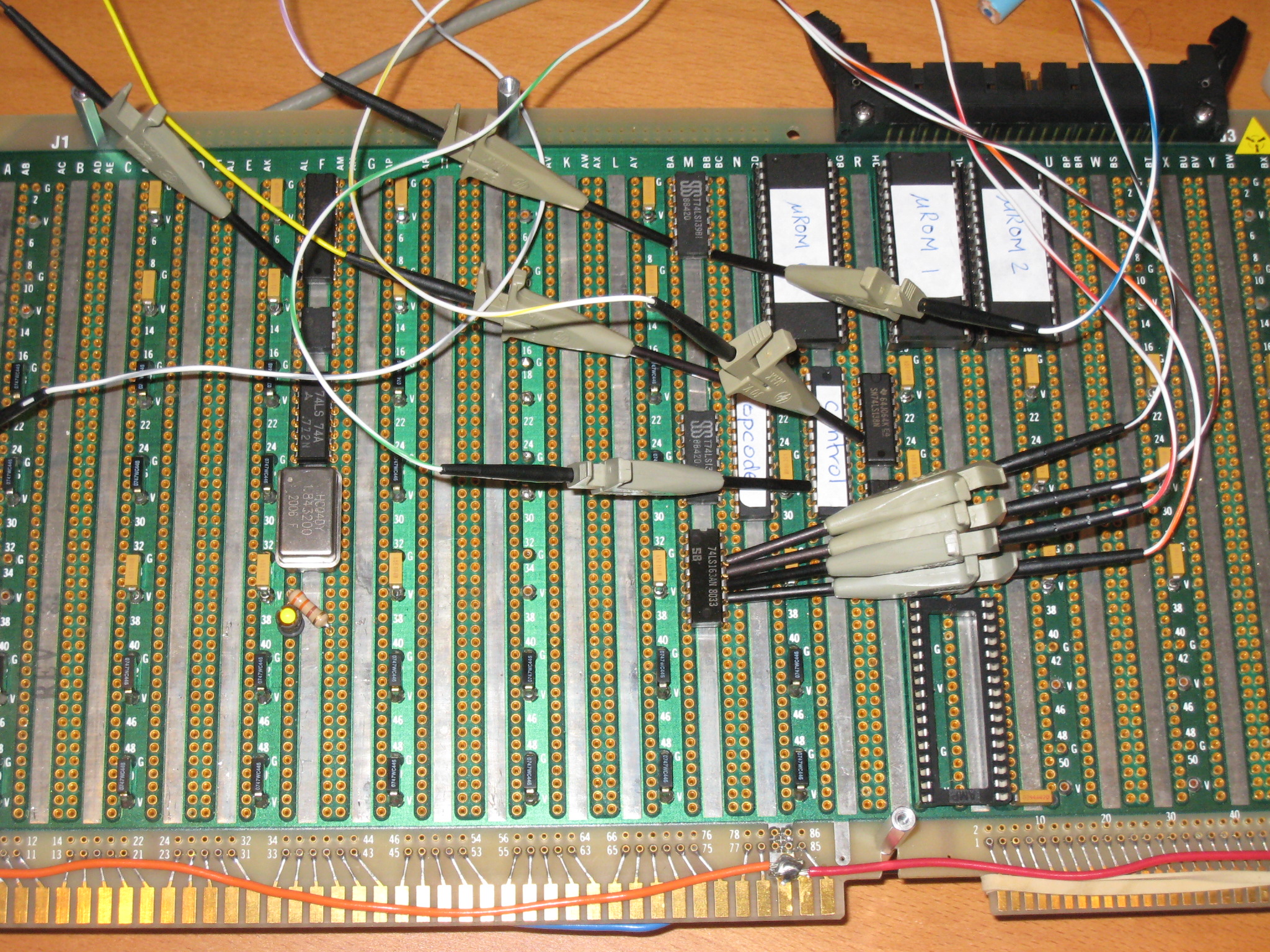
It works!!! Eureka! And on the very first attempt, no less. I have achieved computation from a big mess o’ wires, and a couple of dozen basic logic chips. I can now say confidently that fibonacci(12) = 144. Check out the last line of the logic analyzer data listing:
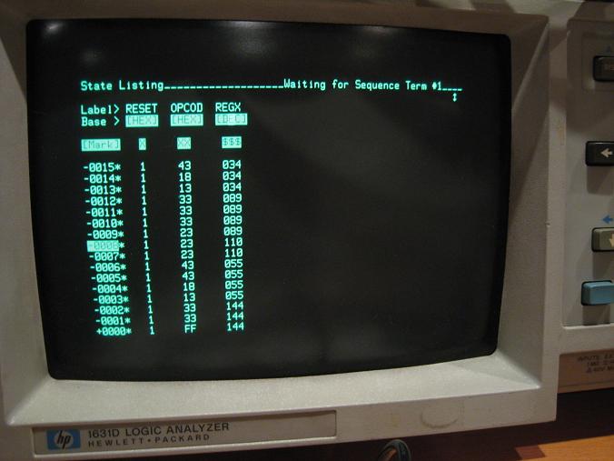
Each line shows the state for a single clock cycle, with RESET (active low, so 1 means normal operation), OPCODE (in hex), and the X register (in decimal). Opcode FF means the machine has halted. You can see the last few terms of the fibonacci sequence on the preceding lines, although they’re not in order, and there’s a random value of 110 there too.
Did I mention that it works? Holy cow. The best part was that mere moments after the successful bootup, a friend called to ask me about something else, so I talked his ear off about the machine.
Since the hardware is still far from complete, running the fibonacci program required quite a bit of chicanery. At the moment there are only two 8-bit registers, and no RAM. The T register was intended to be used for temporary storage by the microcode, and wasn’t meant to be user-visible at all, so I had to add some additional instructions to expose it temporarily. I also added an instruction to add the X and T registers. Then I had to write microcode for a conditional absolute jump instruction, since the hardware needed for a relative branch isn’t finished yet. I had to modify the absolute jump instruction to work only within the first 256 bytes of memory, to avoid disturbing the T register. And finally, since I didn’t have any place to store a running count of how many fibonacci sequence terms had been generated, I resorted to cheating: the program terminates when the sign bit of the X register (bit 7) is 1. So it’s not really computing fibonacci(12), but rather the first fibonacci number >= 128, which happens to be fibonacci(12).
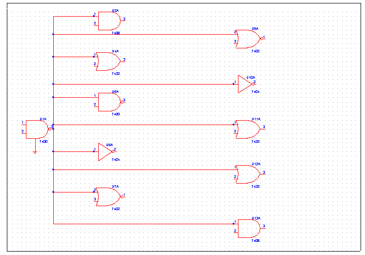
Here is BMOW’s first program:
| * = $0 |
| nop ; let’s hope we can execute a no-op, at least |
| ; load X and T with the first two terms of the fibonacci sequence |
| ldx #1 |
| sxt ; swap X and T, uses XOR swap since there’s no other temporary register! |
| ldx #0 |
| loop: |
| clc ; clear the carry flag |
| axt ; add x + t |
| jmi done ; if the result is “minus” (sign bit is 1), exit the loop |
| sxt ; swap X and T |
| jpl loop ; jump back to the start of the loop |
| done: halt |
Honestly, I’m fairly amazed that it worked on the first try. Yes, I’d been testing the subsystems as much as I could as I built them, but this was the first real integration test. What’s more, it was the first test of any kind that tried to modify the program counter, or use the ALU, condition codes, data registers, databus, or memory bus to data bus interface. I fully expected to spend a long time working out all sorts of problems before getting to the first successful program run. Heck, I must have run into 10 different logic and microcode bugs while testing the fibonacci program on the simulator, and the potential for errors in the impenetrable mass of wires the composes the BMOW hardware is far greater.
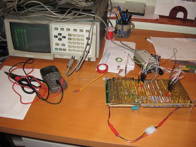
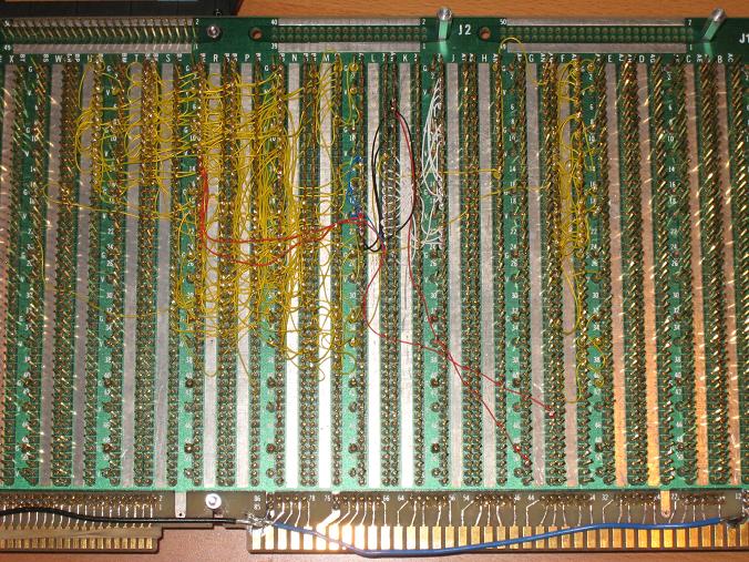
Here’s a look at the testing setup for my moment of glory:
So now I’ve got a very rudimentary computer, with two 8-bit registers and no RAM, running at a blazing 470 kHz. What’s next? I’ll probably write a few more test programs to exercise the hardware in its current state, to make sure everything’s really working as it ought to. Next, I think I’ll try to tackle integrating the LCD module. Checking the progress of the computer with all those logic analyzer probes is not much fun, so it would be great to display “fib(12) = 144” instead. Once I’m able to check the machine’s health without connecting up the logic analyzer every time, I’ll probably move on to the remaining data registers, RAM, stack pointer, and other hardware devices. There’s still a tremendous amount left to do, but as of today, I can finally say I’ve built a working homebrew CPU.
Read 2 comments and join the conversationAlmost There
I’m getting very close to the first real BMOW bootup. I’ve got two data registers wired up, along with enough of the data bus to use them. Now I just need to double-check the current wiring, add the rest of the registers, and see what kind of test program I devise.
My instruction set is copied from the 6502, with some minor additions and changes. In the course of thinking about a good example program for first bootup, a couple of oddities occurred to me for the first time. The biggest one is that there’s no way to add values from two registers. Instead, the ADC instruction always adds the value in the accumulator register to a value in RAM. That’s a problem for me, since I haven’t yet wired up the RAM, but it also seems like a deeper problem. Why wouldn’t you want something like an ADX instruction, to add A + X? Wouldn’t it be faster than a memory access, if the values you want to add are already in registers?
The second oddity is the very non-symmetric nature of the 6502 instruction set. It’s something I was certainly aware of before, but never really thought much about. With these instructions, each register has different capabilities. The results of an add are always stored in A, never X or Y. Indexed memory accesses use X or Y, not A. Only the accumulator can be bit shifted. It all seems arbitrary and awkward, although I’m sure there were good reasons for those limitations in the original 6502 hardware.
All this has got me thinking that maybe I ought to pattern the BMOW instruction set from the 68000, or MIPS, or something else that’s a little more rational. There’s nothing specifically tying BMOW to the 6502, and with a reprogramming of the microcode, I can implement any instruction set I want, as long as it can be realized on the BMOW hardware. For the time being I plan to stick with the current instruction set, though, since I’ve already written most of the microcode, and got a working assembler too. Writing a new assembler is something I particularly don’t relish.
Musings on instruction sets aside, the BMOW construction and wiring is proceeding smoothly, and I probably have more than 50% of it finished now. A lot of things like devices and the stack pointer aren’t strictly necessary in order to run simple programs, so I hope to have some good news about my first bootup with a real program very soon.
Be the first to comment!Straight Line Code
Believe it or not, I think this pig may actually fly! Things are starting to get interesting. After several more days of wiring, I’ve reached the point where I can execute straight line code (no branches or jumps), with no RAM, and no registers. If you think about it for a moment, you’ll realize that given those restrictions, you can’t really do anything with the computer at all. There’s only one piece of state (the current program address), and there’s no way to change that state other than by sequentially executing instructions. It may even be a stretch to say that it’s “executing” instructions, when they don’t change any state. All the instructions might as well be NOPs.
Despite the outwardly boring appearance, I’m actually very happy with this result. The ability to execute straight line code means:
- The program counter works, because it steps through the program instructions correctly.
- The address bus is wired correctly.
- The address decoder works, because it enables the boot ROM for addresses that are mapped to it.
- The boot ROM is set up correctly, because program instructions are being read from it.
- The external data bus (memory bus) is wired correctly, because instructions are transferred on it to the opcode register.
- The microcode and control system work (although I knew this already from earlier tests).
I didn’t exactly stress test it, but everything seemed very solid and reliable during my experiments, with no weird glitchy behavior at all. The couple of signals I examined with the oscilloscope looked pretty clean.
From here, it’s only a couple more steps before I have something interesting working. I think it’s time to start thinking about my minimal definition of a computer, so I can pinpoint the date of the first successful boot. If I had conditional branching, and two registers, that would be enough to write a simple program to compute a factorial or some such. The result would need to be read out with the logic analyzer, since there’s still no human-readable output, but it would be good enough for me to declare BMOW officially up and running. If all goes well, I should be less than a week away from that goal!
Mmmm, 24 bits of delicious address bus.
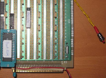
I also managed to cram in a ZIF socket for the boot/program ROM, and a shiny red reset button.
Be the first to comment!Funny Fanout Flaws
Ugh, I’ve run into my first design flaw. Fortunately, I don’t think it will be too difficult to fix, but it’s an eye opener nonetheless.
The issue I’m facing is fanout limitations. Fanout is the number of inputs that are connected to an output. Say I’ve got a chip that outputs some data signal, and that signal is passed as an input to ten other chips, then I’ve got a fanout of 10.
So what’s this about fanout limitations? Can’t you connect as many inputs as you’d like to that data ouput? To understand fanout limitations, it’s necessary to leave the cozy digital world of zeros and ones, and consider the analog nature of the circuit. In the case of a logical “1” at the data output, the output chip attempts to bring the output pin to 5 volts, or something close to it. A small amount of current then flows from the output pin to the input pins. In the case of TTL logic (the 7400 family), as long as the voltage at each input pin is over about 2.4 volts, the input chip will treat it as a logical 1. This allows for a certain amount of loss or noise in the circuit between the output and inputs.
Unfortunately, there is always a small amount of internal resistance in the output chip, between the power supply and the output pin, of something on the order of 10K ohms. Let’s say that an input pin draws 20 uA of current, so from Ohm’s law, V = IR, we can calculate an expected voltage drop of 10KOhm * 20uA = 0.2 volts. So with one input connected, the voltage at the output pin won’t actually be 5 volts, it will be 5 – 0.2 = 4.8 volts. As more inputs are connected, the current will increase, and so will the magnitude of the drop below 5 volts. At some point, if enough inputs are connected, the output voltage will sag below the 2.4v threshold needed for a valid logical “1”, and the circuit will stop functioning correctly.
In reality the situation is somewhat more complicated than I’ve described, as the input resistance needs to be considered too, and in fact TTL outputs never drive all the way to 5 volts anyway due to their design. However, the basic conclusion remains the same: connect too many inputs to a single output, and things will go bad. For TTL logic, the generally accepted limit is 10, although it varies from chip to chip.
Examining my schematics, I realized that they call for 10 different chips connected to my memory data bus, and I plan to add one or two more before the project’s completion. That translates to a fanout of 9 to 11 for each of the bus’ data lines. Maybe that would work fine, maybe not, but I don’t really want to find out. With my luck it would kind of work, some of the time, and I’d never be able to figure out what was going on.
My plan for reducing fanout on the memory data bus is to connect all the “write-only” chips (opcode, LCD, and eventually sound and video) to a 74LS244 bus driver, and then connect that driver to the main memory data bus. That will bring the fanout down to 8, even in the worst case if I do add those extra chips. Isolating the read-only and read-write chips should be possible too if it proves necessary, but it would involve using some glue logic to combine various output enable signals, and bidirectional bus-drivers, and other headaches I’d just as soon avoid if I can.
Be the first to comment!Bit by Bit
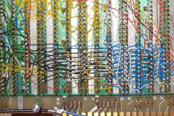
Although progress continues to be slow, the machine is taking shape bit by bit. I bought another 100 foot spool of wire, along with 1000 pre-cut and pre-stripped wires in lengths from 1 to 4 inches. The pre-cut wire makes the job go considerably faster, not only because it saves me from cutting and stripping, but also because consistent length wires are easier to wrap and bend into place on the board.
Big Mess o’ Wires is finally starting to live up to its name! Just look at that mess. My first spool of wire was yellow, and all of the clock and control system connections used the yellow wire. The pre-cut wire I’m using now is a different color for each length: white is 2 inches, black is 2.5 inches, and so on. That gives the board a multi-colored appearance that looks like a mess, but is actually easier to navigate visually than a uniform field of yellow.
The /DRALU problems seem to be gone, now that I’ve made the connections between the ALU system and control system, meaning there are no more floating inputs on the control ROMs. I tested everything out with the logic analyzer again, and it seems OK, although there’s still not much to test with this half-built machine.
At this point, the clock/reset, control, and ALU systems are complete, and I’m getting close to the point where this pile of chips and wires may be able to do something interesting. My next steps will be to add the program ROM, address decoder, program counter, and a few related buffers, and see if I can execute a series of opcodes from the program ROM. Assuming that much works, I’ll add one or two of the registers, and primitive computing should then be possible.
Read 3 comments and join the conversationSlow and Slower
My recent wire-wrapping progress has been painfully slow: I’ve timed myself at about 2 minutes per wire. You might wonder how it could possibly take that long, but all the measuring, stripping, threading, wrapping, and squinting time really adds up. But despite my slow speed, I’m still moving steadily towards a working homebrew CPU.
Yesterday I finished the control section, which is the most complicated part of the CPU. That puts me somewhere in the 25% to 30% range for total CPU completion. As I was nearing the end of the control section, I realized I was running out of wire, and began to worry that I would run out before finishing the last connection. As it turned out, I finished the control section with a bare spool and about 2 inches of wire remaining. Now I’m on a forced hiatus until my replacement wire stock arrives.
The control section by itself doesn’t do much, since there’s no program for it to run, and no registers, ALU, or memory for it to control. But due to some lucky accidents, I was actually able to run and test a program of sorts. Here’s a photo of the setup:
There’s no program ROM, so nothing from which to load opcodes. The opcode register with unconnected inputs appears to default to an opcode of 0xFF, so I programmed the micro-ROMs with a test micro-program for that opcode. My test micro-program exercises all of the various control output signals, which don’t currently do anything. However, I was able to verify their operation with the logic analyzer, and make sure everything is working so far.
I only ran into one problem, with the /DRALU signal that will drive the ALU output. Occasionally it’s a 1 when it should be a 0. More careful examination showed that the bogus 1 value only ever appears immediately after a valid 1, as if it were “stuck” on 1 for an extra clock cycle. The problem also only happens within the first second or two after power-up. After that /DRALU always looks fine, even if I reset the CPU while keeping the power applied.
I also looked at the /DRALU signal with the oscilloscope, and it goes from a nice clean 0 volts for a logical 0, to a nice clean 5 volts for a logical 1, to OH DEAR GOD horrible noise for one clock cycle, then back to a clean 0 volts. So clearly there’s noise that sometimes causes what should have been a 0 to become a 1, but I’m not certain why.
My first guess was a bad/flaky connection on one of the /DRALU pins. However, I can’t see why a flaky connection would only be a problem during the first couple of seconds after power-on, and only during certain clock cycles. And once the machine was warmed up, I wasn’t able to reproduce the problem, no matter how much I jiggled the board, chips, or wires.
My second guess was that I was getting unpredictable behavior, because some of the micro-ROM address inputs are still unconnected. However, the data in the micro-ROM is organized such that the data value will be the same regardless of whether those unconnected address inputs are 1’s or 0’s.
Once I get more wire, I plan to connect up the remaining unconnected micro-ROM address inputs, and see if the problem goes away. If not, I’ll try cutting out and re-wrapping the wires that carry the /DRALU signal. If that still doesn’t fix it, then I’m going to be in for some difficult debugging.
Read 5 comments and join the conversation