

Archive for the 'Bit Bucket' Category
Electronic Junk Mail Teardown
I recently got some very surprising junk mail that contained a full-fledged embedded computer. This was a first for me, but I wonder if there will be more to come? Of course I couldn’t resist the temptation to tear it apart and see what was inside.
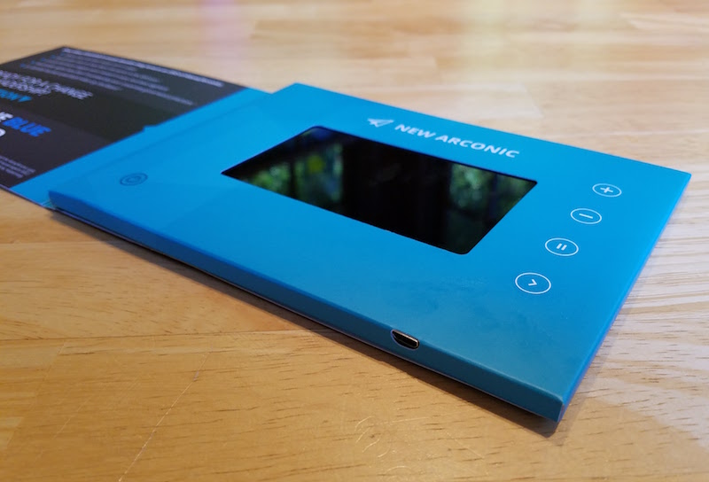
The mail was something related to “The New Arconic”, which appears to be a proxy fight over control of the Arconic corporation (formerly Alcoa, the Aluminum Company of America). They want me to vote for new candidates for the board of directors – blah blah boring. But instead of sending me a persuasive letter or glossy brochure, they mailed a purpose-built video player with a 3 inch TFT screen and control buttons built into a small cardboard envelope.

Nothing happened when I pressed the power button. Dead battery? I located a micro-USB connector on the side, plugged in a charger, and waited. After a few minutes, the distinct aroma of fried electronics began to fill the air, and the cardboard was extremely hot. Doh! Of course, the only thing left to do was tear the paper apart and see what was inside.
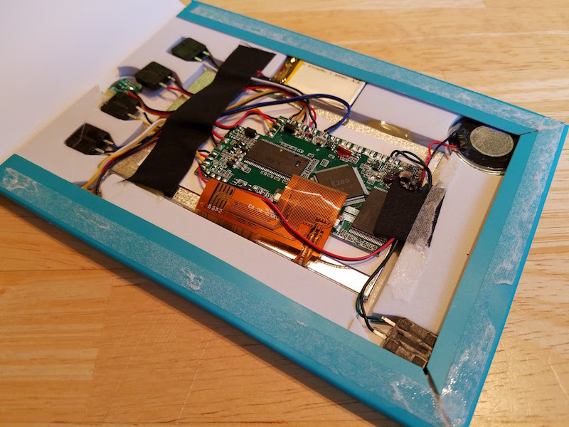
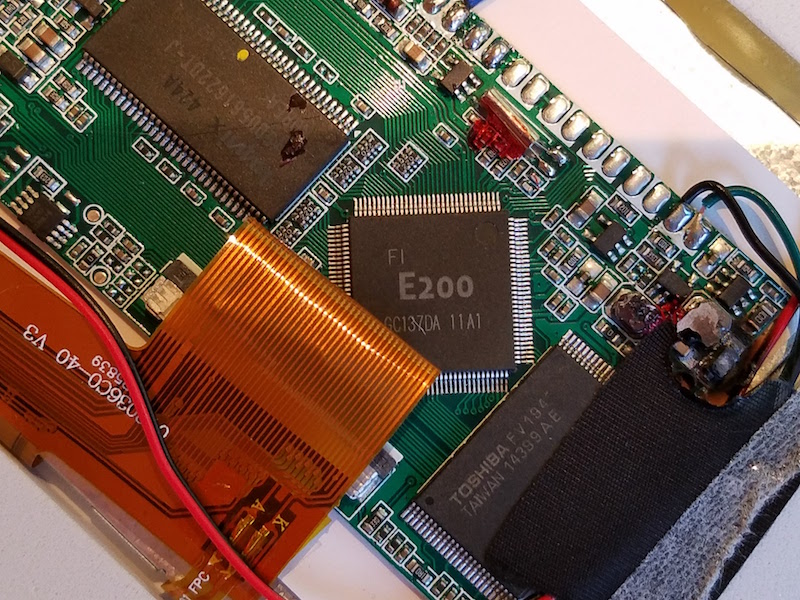
The guts contained a TFT display module, with a piece of paper glued to the back, and a small circuit board affixed to the paper. Everything was connected by point-to-point wiring, and appeared to be hand-soldered. A 500 mAh 1.85 Wh LiPo battery powered the system. Five standard 12 mm tactile switches were taped around the edges, and a circular element in the corner I’m guessing was a piezo speaker. The only component I couldn’t identify was a tiny circuit board containing a single 3-pin chip, attached to a 1cm circular metal disk. It’s labeled Q5, and I’m guessing it’s the transistor used to enable power to the main board. [It’s actually a magnetic relay that turns on the power when you open the box cover.]
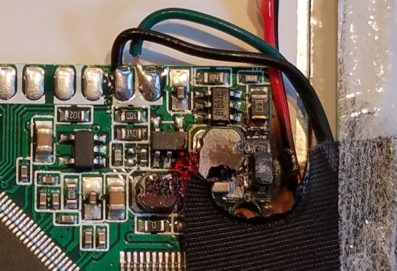
The burnt part of the circuit was clearly identifiable, in a corner of the main board near what looked like two inductors.
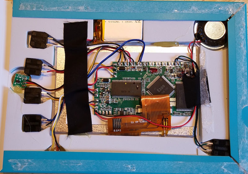
The main board contained three large chips: a Toshiba FV194 14399AE, a Hynix _Y5DU561622DT-J, and an unbranded E200 GC137DA. The first letter of the Hynix part number was obscured by burnt crud. I couldn’t find any info on the Toshiba chip, but based on its appearance and by process of elimination I’m guessing it’s a flash ROM containing the video file to be played. The Hynix part is DRAM of some type, though I couldn’t find an exact match on the part. The E200 is a PowerPC based system-on-a-chip. While searching for info about it, I found this Hackaday article from 2014 describing a teardown of very similar hardware. It looks like this is a standard platform for disposable electronic advertising, and the Italian company that makes them is here.
Given that they mailed me a fire hazard that needs to be specially recycled, I’m not too sympathetic to New Arconic’s advertising.
Managing Multiple Power Supplies
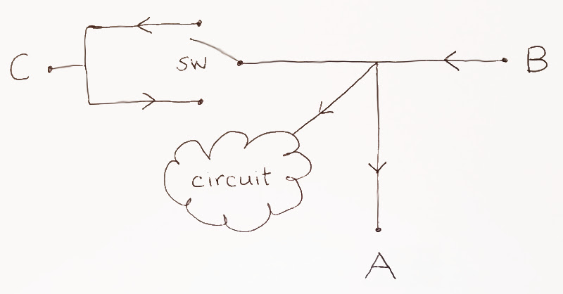
I’ve been investigating ways to handle multiple supplies and consumers of +5V 500mA power in a single project, and it’s surprisingly complicated. My circuit may have up to three simultaneous external connections: a device needing +5V power at “A”, an external +5V supply at “B”, and something at “C” that might either supply +5V power or need +5V provided to it, depending on what mode the circuit is operating in. Any of these three could be present or absent, and the external +5V supplies could possibly be connected but turned off and not delivering power.
The simple solution would be to directly connect all of those +5V lines within my circuit. That would work, and maybe it’s what I’ll do, but it presents some risks of unintended current backflow into a supply. Imagine if B and C are both connected, with C configured as a supply. If one is turned off, the other would feed +5V into it. Depending on what that supply is and how it’s designed, feeding external +5V back into a device that’s turned off may cause weird behavior or damage. A similar problem could arise if a poorly-designed device on A actually powers the +5V line instead of drawing power from it, because it has batteries or an independent supply of its own.
I’m willing to handle the bidirectional nature of C with a physical switch. But I still need something that ensures current only flows in the intended direction in/out of A, B, and C, as shown in the diagram above. The ground connections aren’t shown, but they are all tied together. Current direction arrows mean diodes, right? I think diodes would theoretically work, but probably aren’t the best choice. A diode would cause a substantial voltage drop between the supply and whatever it was powering, and you need a diode that’s physically large in order to handle significant amounts of current.
A better solution might be a transistor. From studying similar circuits, a good choice might be a power MOSFET. These have a very low resistance when switched on, resulting in only a small voltage drop. A small-sized MOSFET could also handle all the 500mA current I need for this project. But I don’t have any experience working with single MOSFETs in this kind of application. I get a bit bogged down in discussions of N and P type, enhancement and depletion, high-side and low-side switching, and so forth. I’m not completely confident I’d know which specific MOSFET to select for my purpose, and how to connect it in the circuit, and what limitations or unexpected behaviors it might have.
An even better and simpler solution might be a power distribution switch IC, like the Microchip MIC2005A. This is basically a MOSFET, but one that’s designed for this specific purpose, with some extra features like soft start, current limiting, and thermal protection. And in the SOT-23 package I’d likely use, it’s not much more expensive than a generic MOSFET.
Power distribution ICs are designed to conditionally enable a power supply, and they have an /ENABLE pin to determine when to energize OUT from the supply at IN. But I would be using them always enabled, just to get the reverse current protection feature. Maybe that means this is the wrong tool for the job, and a different solution would be better?
A second question is whether a power distribution IC like the Microchip MIC2005A actually provides reverse current protection. It has terminals labeled IN and OUT, but it’s not clear if anything prevents current flowing from OUT to IN if OUT is energized by something else. I skimmed the datasheet, but couldn’t find any mention of this.
A final question is whether connecting the OUT terminals of several MIC2005A chips would cause problems. That’s what I’d need to do, if both B and C might function as +5V supplies. I can imagine this might cause a problem if one of the MIC2005A chips finds its OUT terminal at +5V even though its IN terminal is at 0. Or it might be a problem if both B and C were turned on at the same time, both delivering “5 volts”, but one was 4.9V and the other 5.1V. I didn’t see anything in the datasheet that addresses this either.
I’m trying very hard to keep the total cost of this solution low, like 50 cents or less. There are more complex power management ICs that might simplify things, but cost $2 or more apiece. Add the cost of assembly, and a retail markup sufficient to get acceptable margins, and the final sales price of the product would have to be increased by an unacceptable amount. I would probably choose to eliminate functionality instead, or just use the “connect all +5V supplies” approach, before I made a significant increase in product price just to support power management.
My diagram shows five current direction arrows, so potentially I would need five MOSFETs or MIC2005As. But I don’t actually need one on the line to the “circuit” cloud, because there’s no possibility of current flowing the wrong way. And the two arrows at C could probably be collapsed into a single arrow, if I used a DPDT switch that reversed the connections to the MOSFET or MIC2005A terminals. And I maybe don’t really need the arrow at A. If a device at A were to backflow +5V power, it would turn on the circuit, and possibly also supply power to C depending on the switch setting. That would be unexpected, but I don’t think it would harm anything. Applying all those simplifications, I might be able to get away with as few as two MOSFETs or MIC2005As, squeaking under my arbitrary $0.50 budget.
Read 21 comments and join the conversationFruit + Electronics = Piano
The human body is electrically conductive. A piece of fruit will also conduct electricity, as will basically anything else that’s organic. We can leverage this fact to create a fun little afternoon project: a digital fruit piano. No soldering is necessary, and the whole thing takes less than an hour, even for a total beginner like my 9-year-old daughter. What sound does a banana make? Let’s fine out.
While humans and fruit do conduct electricity, they’re pretty bad at it. Both typically have an electrical resistance that’s in the 1-megaohm range, depending on how moist your skin or nectarine is. This design uses your body and the fruit as part of the circuit, flowing current through the human-fruit “wire”, but the high resistance means that the currents involved are tiny. The piano player isn’t going to feel a shock, or even feel anything at all. She’ll just lightly touch different bits of fruit to play a song, almost as if by magic.
This isn’t my original design. The idea of controlling a digital device by using the human body as part of the circuit has been around for quite a while, and the Makey Makey has popularized it with a nice little kit. If you like this type of project, definitely check out the Makey Makey! But if you’re lazy and cheap like me, you can build a similar device yourself with only an Arduino and some hookup wire, a few resistors, an audio speaker, and a selection of bananas, pears, and peaches.
How does it Work?
The basic concept is simple. Each piano key is a voltage divider circuit involving two resistors: one 1-megaohm resistor and one piece of fruit. Touching the fruit will change the resistance in the circuit, resulting in a change to the voltage at the junction between the two resistors. The Arduino can measure this changing voltage with an analog input, and use it to control an audio speaker.
To complete the circuit, one hand should be connected to the Arduino’s ground pin, while the other touches the fruit. Current will flow through one hand, up the arm, across the chest, down the other arm, and back to Arduino GND. For convenience’s sake I connected GND to a metal ruler, but a plain jumper wire also works fine. For the fruit connection, just stab a wire straight into the fruit. Soldering a banana works poorly…

If the hand isn’t touching the fruit, then the whole fruit-hand-body section becomes an open circuit with infinite resistance. In this case, the circuit simplifies to just +5V connected through a 1 meg resistor to the analog input. Because the analog input draws virtually zero current by itself, there will be no current flowing in the circuit and no voltage drop across the 1 meg resistor (remember Ohm’s law V = iR, so when i = 0 then V = 0). The voltage measured at the analog input will still be +5V, and Arduino’s analogRead(A0) function will return 1023, the maximum possible value for its 10-bit resolution.
When the hand touches the fruit, the fruit-hand-body section forms an organic resistor of about 1 megaohm. Current will flow from +5V through the real 1 megaohm resistor, then through the fruit-hand-body 1 megaohm resistor and down to ground. The total resistance between +5V and GND is 2 megaohms, and with two equal value resistors, the voltage at the point midway between them will be half the total voltage drop. That means the Arduino’s analog input will see 2.5V, and the analogRead(A0) function will return a value around 512.
To make a piano, a simple Arduino program is needed to continuously poll each analog input, and play a tone if the analog value is below an appropriate threshold. I used a threshold of 800, but you’ll need to experiment to find the value that works best for you. The sample program uses tone frequencies corresponding to the notes CDEFGA of a C major scale, making it easy to bang out favorites like Mary Has a Little Lamb, Hot Cross Buns, and I Ate the G Key.
Each of the six fruits is connected to one of the six Arduino analog inputs A0 to A5. If you’re wiring this up at home, duplicate the pictured banana circuit six times, connecting the first to A0, the second to A1, and so on up to A5. Then connect your speaker’s black wire to GND and red wire to Arduino pin 8. Happy fruit playing!
void setup() {
}

void loop() {
  if (analogRead(A0) < 800)
  {
    tone(8, 523, 130);
    delay(80);
  }
  else if (analogRead(A1) < 800)
  {
    tone(8, 587, 130);
    delay(80);
  }
  else if (analogRead(A2) < 800)
  {
    tone(8, 659, 130);
    delay(80);
  }
  else if (analogRead(A3) < 800)
  {
    tone(8, 699, 130);
    delay(80);
  }
  else if (analogRead(A4) < 800)
  {
    tone(8, 784, 130);
    delay(80);
  }
  else if (analogRead(A5) < 800)
  {
    tone(8, 880, 130);
    delay(80);
  }
}
Battery-Powered Apple IIc, Part 2

This funny-looking device is a DC barrel plug to Apple IIc DIN-7 adapter, inspired by last week’s musings on constructing a battery-powered IIc. The adapter makes it possible to power an Apple IIc with a standard DC supply between 9V and 20V, or a suitable battery pack with a DC plug. The supply or battery should be capable of delivering at least 20 watts, or about 1.67 amps at 12V.
For my experiments, I used a Belkin BU3DC001-12V, which is essentially a fancy 12V 7.2Ah battery with built-in charging circuitry, output regulation circuitry, and fuse. It’s intended to be a backup battery for VOIP systems, but can easily be repurposed for any 12V DC application. Best of all, it’s only about $20 used, which is hardly more than the cost of the battery itself.
The current draw estimates from my earlier post proved to be about right. When running from the 12V battery, the IIc pulls about 1.5 amps for a few seconds while the floppy drive spins. Once the drive stops, the current drops down to about 700 mA. Given the 7.2 amp-hour capacity of the Belkin unit, that ought to be enough for several hours of battery-operated IIc fun.
Building your own DC to IIc adapter is simple, and only requires some wire and a few dollars in parts.
Female DC Jack to Screw Terminal Connector – $1.99
DIN 7 Pin Plug Set – $6.21
Video
If you’re wondering why there’s no funny video here of a IIc running in the woods, it’s because I’ve only solved half the problem. A battery-powered IIc is pretty useless without a battery-powered monitor to use with it. Fortunately, 12V DC powered LCDs with a composite video input aren’t difficult to find. Many portable DVD players and car entertainment systems can do that job. To power it, I could build another custom cable to run the monitor and the Apple IIc off the Belkin battery, but I’m going to be lazy and simply buy this splitter:
12V Splitter Cable – $6.59
It remains to be seen how much current the monitor will draw from the battery, but hopefully not much. I’ll report again when I have solid numbers.
While I already have a portable DVD player that will work here, its 5 inch diagonal is a little bit underwhelming. I also have a much nicer 14 inch LCD monitor that runs from 12V DC, but it only has a VGA input and no composite input. I’ll keep my eyes peeled for an LCD that’s 9 inches or larger, running from 12V DC, with a composite video input, to create the ultimate battery-powered Apple IIc system. Then I can… um… OK, I admit there’s no real point to this project. 🙂
Read 3 comments and join the conversationBattery-Powered Apple IIc?

I’ve got the crazy idea in my head to run an Apple IIc system completely from battery power, so I could take it on the road. I know it’s possible – there’s already one person selling a pre-made kit. That’s a nice solution, but the pictured setup involves an automotive jump-start battery that costs around $150. Would something simpler be possible?
The Belkin Residential Gateway Battery Backup pictured above is designed to keep your VOIP phone or similar device working during a power outage, but it’s found a second life as a popular portable 12V supply for electronics projects. Inside the Belkin unit is a 12V/7.2Ah lead-acid battery. It charges from a standard AC wall outlet, and has a DC barrel plug for connection to the powered device. Hack that off and attach a 12V car cigarette lighter receptacle, or other connector of your choice, and you’ve got a nice little portable power source.
Is 7.2Ah enough to do anything interesting? To answer that question, we need to know how much power an Apple IIc requires. My Apple original AC adapter says it outputs 15V @ 1.2 amps. The IIc can accept any DC voltage between 9V and 20V, so the Belkin’s 12V should be fine here. 15V @ 1.2 amps is 18 watts, and to get the same power at 12V we would need 1.5 amps. That tells us the maximum power the AC adapter can deliver, based on what’s printed on its case.
What about the average power? That’s much more relevant, if we’re trying to estimate the possible run time while connected to a battery. I used a Kill-a-Watt to measure the AC adapter’s power draw from a wall outlet, and it was 12 watts while the IIc was idle doing nothing. So the adapter draws 12 watts from the wall, and delivers something less than 12 watts to the IIc, depending on its efficiency. I don’t know if it’s a switching regulator, or how efficient it is, but I’ll be generous and assume it’s 75% efficient and delivers 9 watts to the IIc. If my reasoning is correct, that means a IIc at idle would draw 0.75 amps from a 12V battery (9 watts).
Back to the Belkin unit: its 7.2Ah battery should theoretically be good for 9.6 hours of runtime, assuming the average power draw of the IIc is close to the idle draw of 0.75 amps. 9.6 hours seems a bit hard to believe, but I’ll go with it for the moment.
Now what about a monitor to use with the computer? Fortunately I’ve got an old portable DVD player with a composite video input that I know works with the IIc. And the DVD player runs off 12V! I haven’t measured its power draw, but I don’t think it can be more than the IIc itself. I’ll assume it’s equal to the IIc’s draw, so the total battery runtime of a IIc with DVD player / monitor would theoretically be 4.8 hours.
If the Apple IIc used any type of standard DC power connector, I’d give this a try right now. Instead, I need to go digging for a female DIN-7 plug. Why must every vintage Apple system include some kind of obscure connector? 🙂
Read 15 comments and join the conversationDirty PCBs Review

Today’s electronics hobbyists are blessed with many options for custom PCB manufacturing, like Seeed, Elecrow, and OSH Park. For around $1 to $2 per board, depending on size and quantity, these vendors will turn your EAGLE or KiCad or other Gerber files into shiny new PCBs. I’ve used all three in the past, but my go-to vendor for most things is Seeed.
Dirty PCBs is a newer entry in this space, but it’s affiliated with Dangerous Prototypes, who are long-time members of the hobbyist electronics community. A few years ago Ian Lesnet moved himself and the company to Shenzhen, China, and Dirty PCBs is sort of a matchmaking service between Shenzhen PCB manufacturers and hackers around the world. For a recent PCB purchase of 20 boards, I decided to give them a try.
Saving Pennies
The main attraction of Dirty PCBs is the price. Even among other cut-rate PCB manufacturers, it stands out as the cut-ratest. Any color PCB is available for the same cost, whereas most manufacturers charge extra for colors other than green. Slow-boat shipping is free worldwide, and the faster shipping options tend to be cheaper than at the competition. For my order of 20 red PCBs, 10×10 cm size, shipped by DHL China, here’s how Dirty PCBs compared to Seeed:
10×10 cm PCB @ qty 20 = $57.43
Red soldermask = $10.00
DHL shipping to USA = $24.71
TOTAL = $92.14
Dirty PCBs
10×10 cm PCB @ qty 20 = $50.00
Red soldermask = $0.00
DHL shipping to USA = $15.00
TOTAL = $65.00
Dirty PCBs also uses a constant price per board as you increase the quantity, or offers a small discount for larger quantities, as you would typically expect. Seeed has the bizarre habit of offering a negative “discount” for higher quantities. E.g. with Seeed it’s sometimes cheaper to buy 10 boards twice than to buy 20 boards.
Ordering
My biggest gripe with Dirty PCBs is the website itself and the way it’s marketed. The site’s tagline says “No bull, just crappy PCBs.” I suspect I’m in the minority, but I just don’t appreciate the joke here. Call it basic, no-frills, or rock-bottom if you like, but please don’t tell me I’m paying money for something that’s intentionally crappy. Especially when, if you read the specs and the terms, it’s not crappy at all. Yet I’m somehow left with a mental picture of a sloppy, careless, and all-around half-assed manufacturing process. I don’t think it’s accurate, but that’s the image it paints in my mind.
To be fair this attitude is intentional, and can be traced to the “accidental” launch of the Dirty PCBs service. As Ian tells it, he never meant to launch a PCB service, but simply hacked together some scripts for the convenience of his friends. That unofficial “for friends” service became unexpectedly popular, and Dirty PCBs was born. Ian’s said in the past that the service doesn’t really make any profit, so his tolerance for whiners and time-wasters is low. To quote the About page:
This site was intended for friends and not the public. We’ll process your boards, but we only make about 30 cents per order. We really don’t care if you want to take your business somewhere else, and it’s not worth our time to deal with stupid questions or asshats. Paypal fee reversals, annoying emails and the like will get you banned from the site.
Fair enough, and +1 for use of the word “flippant”. The actual ordering process was simple, except for a mistake I made when uploading the Gerber files. The upload button doesn’t mention what file format it expected (I later found this information on the About page), so I uploaded a zip archive of the same Gerbers I would normally send to Seeed. It appeared to work, and I went through the entire checkout and payment process, only to be informed after I’d paid that no board outline file was found. This was because my Gerbers had different filename extensions than Dirty PCBs was expecting. After renaming the files and uploading a new zip archive, all was well.
Delivery
My order was placed on Thursday afternoon, and the finished PCBs were in my mailbox on the following Wednesday afternoon. Six days! That is crazy fast. Maybe I just got lucky and hit the manufacturing cycle at the perfect time, but that’s more than twice as fast as any other PCB order I’ve ever made in China or the USA.
Inside the box was an unexpected surprise – 23 PCBs instead of 20. I know the Dirty PCB’s proto-pack is “about 10” and often 11 or 12, but I didn’t realize they did a similar thing for larger orders. Presumably they make 10% extra in case some PCBs fail the e-test, then mail you all the boards that passed testing. So hey, three extra free boards. Thanks!
Inspecting the Boards

Now for the key question: were the boards any good? From my inspection, I’d say mostly yes. I spent a long time examining the boards under 10x magnification, and comparing them to my original EAGLE files, and to the Gerbers using gerbv. Probably I’ve never examined any PCB quite so intensely, and some of the issues mentioned below may be typical of other discount PCB manufacturers too. For the money paid, I’m not complaining, but for completeness I’ve catalogued the good and the not-so-good.
The Good
First and foremost, my sample PCB worked great once I populated the components and put everything together. This is about the only thing that really matters in the big view, and it means there were no accidental shorts or breaks in the PCB traces. Of course I hadn’t really expected any problems there, since Dirty PCBs advertises a minimum 5 mil trace/space size, but I only went down to 8 mil and was nowhere near the limit.
My board is a rather funky hexagon shape, or a triangle with clipped corners if you prefer. There were no problems routing this non-standard board outline.
When examined under magnification, all the drill holes appeared nicely centered in the vias and pads. The edges of traces and planes appeared clean and crisp. Silkscreen was sharp and nicely legible. The soldermask was a nice bright red color, and tented vias were actually tented.
The Not-So-Good
One small gripe: the silkscreen layer was slightly offset from the copper layers and drill holes, as you can see in the photo below. The silkscreen outline for this AVR ISP footprint isn’t centered around the pads. This doesn’t matter much, but it may bother you if you’re a stickler for little details.

One bigger gripe, that I’m still not sure is my fault or Dirty PCBs’ fault: some of the extra-large vias appear either larger than intended, or not in the right place – it’s hard to be sure which. Here’s an example of a large untented via that connects ground planes on the top and bottom of the board. In the photo, notice how the edge of the drill hole is almost exactly in line with the edge of the ground plane (which is partly obscured by the silkscreen line)? And the plating around the drill hole actually extends beyond the ground plane, bowing outwards slightly into the gap between the ground plane and the neighboring trace? And the stop area (the area without soldermask) extends nearly all the way to that neighboring trace?

Here’s the same region viewed in EAGLE, with the silkscreen hidden. Notice that the drill hole comes well short of the ground plane’s edge, the plating around the hole doesn’t extend beyond the edge, and the stop area only extends maybe one-third of the way into the gap between the ground plane and the neighboring trace.

And here’s the same region once more, looking at the actual Gerber files with gerbv. The top copper layer is magenta, drill holes are lavender, and the stop mask is gray. Maybe the Easter Bunny chose this color scheme. Where layers overlap you’ll see additive coloring. There’s no separate color for the plating around the hole here, since both the plating and the ground plane are just part of the top copper layer. It almost looks like Dirty PCBs interpreted the stop mask layer (gerber.GTS) as an additional top copper layer, than generated its own stop mask around that.
Another possibility jumps to mind as I type this: I used a non-standard drill size for those extra-large vias of 0.02362205 inches – not sure how that happened. I wonder if DirtyPCBs rounded up to the next larger drill size, then automatically enlarged the copper area and stop mask to compensate. The through-hole pads in these pictures use a 0.040 inch drill, so the ratio of the hole sizes should be 0.02362205 / 0.040 = about 0.59. But measuring the actual hole size ratio observed in the PCB photo, it’s about 0.62. So those via holes are about 4.7% larger than they were intended to be, if my figuring is correct.

Here’s another example of the same issue. This via bulges outward slightly from the top-left of the ground plane, and the stop area extends all the way to the neighboring trace. But in the source file, the via’s drill hole and plated area are both completely within the boundaries of the ground plane, and the stop area only extends about a quarter of the way to the neighboring trace.

Overall Rating
As an overall rating, I’m giving Dirty PCBs a thumbs-up. They were cheap, super fast, sent me extra boards, and the boards worked. I’m not sure I’d trust them yet with a design that goes all the way to the 5 mil limit, but it’s probably best to avoid that limit anyway. I wish they’d change the name or at least the tagline, but that’s just me. I expect I’ll use Dirty PCBs again, and will report how it goes. Thanks for reading!
Read 6 comments and join the conversation