First Simulation
It simulates! I completed the Verilog description of the machine, and after fixing one place where I’d used an active high instead of an active low enable single, it worked like a champ. I implemented the microcode for NOP, JMP (absolute), and HALT. I was able to run this simple program from ROM: NOP
LOOP: NOP
JMP LOOP
Of course I don’t actually have an assembler or any other software tools, so I couldn’t write the program symbolically like this. My test program is just a bunch of hex numbers entered by hand into a text file. That’s marginally tolerable for a 5-byte assembly program, but writing microcode that way gets old very, very quickly. Each line of microcode is 24 bits wide, and keeping track of what every bit means in my head, for every line of microcode in even a simple instruction like JMP, is near impossible. I need to write a quick-and-dirty microcode assembler before I go any further.
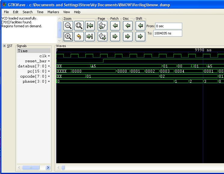
Here’s a simulation trace of the machine booting up and executing the above program.

I used the awesome free tools Icarus Verilog for compiling and simultating, and GTK Wave for analyzing the waveform results. I put basic timing information into the hardware model as I was constructing it, using Verilog delays to make outputs lag inputs by the worst-case propagation delay cited in the datasheet. Theoretically, I should be able to use this to determine a lower-bound on the machine’s clock speed: just crank up the simulated clock speed until it stops working.
While completing the Verilog description of the machine, I found that I needed more “glue logic” chips for computing simple boolean functions than I’d like. Decoding memory addresses to enable the appropriate memory-mapped hardware required three different chips, and I needed several more to help with hardware initialization signals during reset. I ended up needing at least one each of NAND, NOR, AND, and OR. If I were more clever, I think there’s a lot of opportunity to clean up this logic and reduce the required chip count. Maybe I should look at using a PAL (or PLA? are they the same thing?) to compute all my simple boolean functions on a single chip, although it might be a lot slower.
I had an idea for a way to add a Y register to the machine, with just two more chips: a ‘377 register and a ‘244 driver. The obvious place to add it as at the right ALU bus, where there are presently only 3 inputs, but the control ROM encoding allows for 4. The problem is that the control ROM only allows for 8 “load destinations”: A, X, T, PCLO, PCHI, ARLO, ARHI, MEM. My idea was that I could have ARLO chain-load from ARHI instead of from the data bus, with just a single load enable signal instead of separate lo/hi enables. That would free up space for a Y load enable. Of course it would mean the machine could never load ARLO and ARHI independently: it would always have to load them one after another, first ARLO, then ARHI. I’m not sure if that’s practical, and I suspect it may not be, at least not without a performance penalty.
Construction update: I’ve started looking further into how to assemble this thing. I’m planning to use wire-wrap construction, even though I have no experience with it, since it seems like that’s what everyone else does. I found some used wire wrap tools and boards on eBay, and I’ll try to pick up something cheap. I’m not sure yet what I’ll mount the board inside. Maybe an old PC case, or a vanilla plastic project case, or a wooden box. It needs to be something to which I can mount some LED displays, switches, and buttons, with a little bit of homebrew bling, even if it doesn’t look like the bridge of the Enterprise.
Read 1 comment and join the conversation1 Comment so far
Leave a reply. For customer support issues, please use the Customer Support link instead of writing comments.


[…] Extra Data Register: A while ago, I considered adding a Y register to the machine, but ran into the limit of 8 possible load destinations. Now that I’ve increased the limit to […]