Retro USB 1.1 Fail

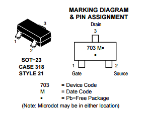
I received a large number of new Retro USB PCBs today, which include a few small component changes from the 1.0 design. Bad news: I blundered by reversing the gate and drain connections on the MOSFETs used for level conversion. DOH!! Always read the datasheet carefully, boys and girls. On a 3-pin device, I must have assumed the gate would be the pin on the side by itself, with drain and source paired up on the other side, just like the canonical drawing of a transistor. Unfortunately that’s not true here. Hopefully I can find another brand of SOT-23 N-channel MOSFET whose pins are organized the way I thought they should be, or else this whole pile of PCBs is going into the trash. For a moment I thought maybe I could rotate the MOSFET 120 degrees, or even mount it upside down, but I don’t think any soldering tricks can save me.
Read 5 comments and join the conversation5 Comments so far
Leave a reply. For customer support issues, please use the Customer Support link instead of writing comments.


Every manufacturer appears to use the same pin layout for 3-terminal SOT-23 MOSFETs, so I think I’m out of luck.
There’s a JFET with the pin organization that I need: http://www.onsemi.com/pub/Collateral/MMBFJ309LT1-D.PDF I’m not very familiar with JFETs though, and I’m not sure one would work here. The bidirectional MOSFET level-shifter relies on the presence of a body diode, among other differences.
bodge wire never killed anyone 😉
Well, it depends on the device you’re replacing. If it’s a 2N7002 Enhancement MOSFET or similar, a depletion mode JFET will not work in its place.
Good news: a couple of extra wires and some creative soldering are enough to get the v1.1 board working. It’s slow and tedious, but better than throwing the PCBs in the trash bin.