Yellowstone JTAG Debugging
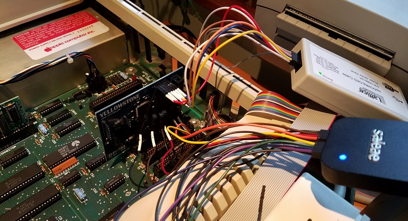
After a month of inactivity, I finally returned to my unfinished Yellowstone disk controller project to investigate the JTAG programming problems. Yellowstone is an FPGA-based disk controller card for the Apple II family, that aims to emulate a Liron disk controller or other models of vintage disk controller. It’s still a work in progress.
Last month I discovered some JTAG problems. With the Yellowstone card naked on my desk, and powered from an external 5V supply, JTAG programming works fine. I can program the FPGA to blink an on-board LED. And when I insert the already-programmed card into my Apple IIe and power it from the slot, it works – the LED blinks. But if I try to do JTAG programming while the card is inserted in the IIe, it always fails with a communication error. I’ve run through several theories why:
- It might be some kind of noise or poor signal integrity on the JTAG traces. But the traces are quite short and don’t cross any other signal traces that might carry interfering signals.
- Maybe I have power problems, and the IIe’s 5V supply is drooping briefly when I try to program the FPGA via JTAG. But I measured the 5V and 3.3V supply voltages during JTAG programming, and they look fine.
- There might be a ground loop, due to the Apple IIe and JTAG programming having different ground potentials. But I measured the difference in grounds, and it’s only 4.3 millivolts.
To help solve this mystery, I used the analog mode of my Saleae Pro 8 Logic analyzer. In analog mode, it functions like a simple 8-channel 12.5 Ms/sec oscilloscope. I recorded the 3.3V supply for the FPGA, as well as all the JTAG signals. First, here’s what the first three seconds of JTAG traffic look like when programmed externally:
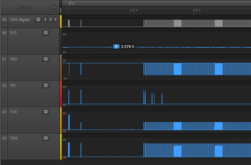
There’s about 1 second of preamble communication, and the rest is the FPGA configuration data arriving at high speed. The 3.3V supply for the FPGA remains at about 3.28V through the whole process. The JTAG signals TMS, TDI, and TDO span the voltage range from 0.17V to 3.2V, which seems fine. But the the TCK signal never goes higher than 1.86V. Uh oh, what’s happening there? Let’s zoom in a little:
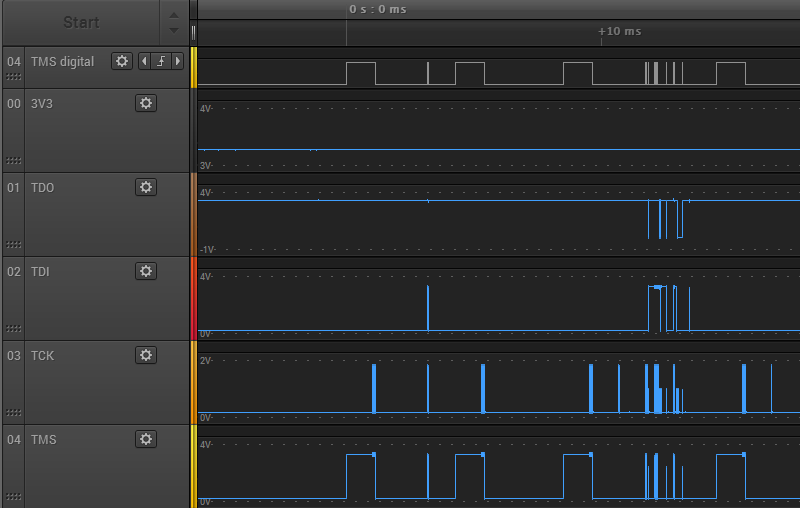
Zooming in, things are even worse than they appeared initially. TCK never climbs above 1.86V, but many TCK pulses only get half that high, stopping at 0.97V. TMS and TDI show some runts too. Zooming in even further on one of the problem areas:
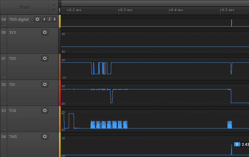
Here you can see a couple of the 1.86V TCK pulses, followed by a whole mess of the runtier 0.97V pulses. Ugh. These should all be using the full range 0 to 3.3V, or something close to it. With a clock signal this bad, it’s amazing the JTAG programming still works.
Do these graphs really reflect what’s happening? I’m a little suspicious that I’m running into limitations of the Saleae Pro 8’s analog mode. At 12.5 Ms/sec, it’s taking one analog sample every 0.08 microseconds or 80 nanoseconds. That’s pretty poor as scopes go, but the period of the JTAG clock is slow: about 1 microsecond (1 MHz operation). There should be 12.5 samples per clock period, more than enough to get a decent reading for the min and max voltage of each clock period. Therefore I think the graphs are accurate.
My conclusion is that although external JTAG program succeeds, the JTAG signals look terrible. The fact that JTAG programming fails when the card is in the Apple IIe slot likely has little to do with the IIe, and everything to do with some other basic signal quality problem.
Next I put the Yellowstone card into the Apple IIe, and repeated my test. Here’s the first three seconds of JTAG traffic again:
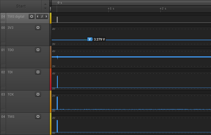
There’s a short bit of preamble communication, then nothing. Something must go wrong at the beginning, and the rest of the communication is aborted. The voltage levels all look about the same as when programming externally. The 3.3V supply is about 3.28V, TCK never goes higher than 1.86V, but the other JTAG signals use the full voltage range. Zooming in, we observe the same extra-runty TCK pulses as with external JTAG programming:
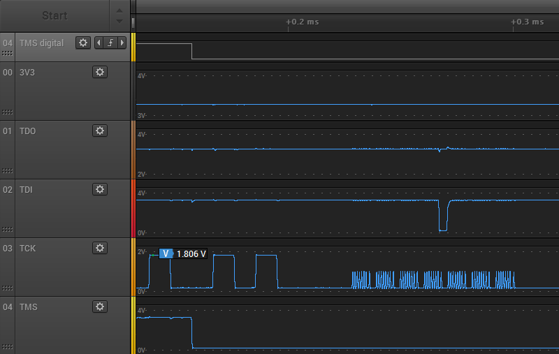
It’s not obvious to me why external JTAG programming succeeds, but programming in the Apple IIe slot fails. Both cases look equally bad. The only real difference I noticed is the TDO signal. In the case of external programming, the TDO high voltage is very steady at about 3.268 volts, and never varies by more than 0.01V. It also drops low at many points during the JTAG communication. But in the case of in-slot programming, the TDO signal is always high and the voltage is noisier. It’s a subtle difference, but you can see the minor noise here:
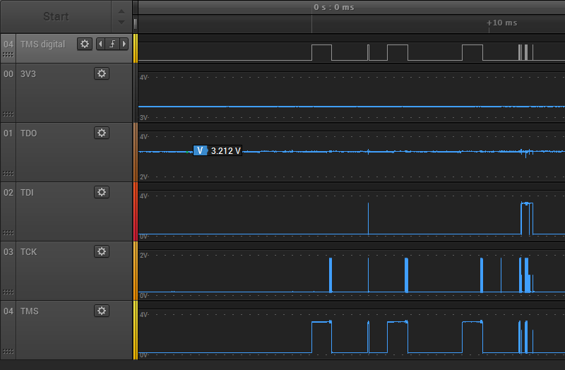
The TDO high voltage ranges from 3.187V to 3.314V, so it’s about 10x noisier than during external programming. It’s still within an acceptable range though, so maybe this isn’t important.
Finding the Culprit
Now that I know I have poor quality JTAG signals, where do I look for the cause? Poor quality JTAG programmer? Bad PCB design? Here’s a section of the PCB, showing the path of the JTAG signals from the connector to the FPGA:
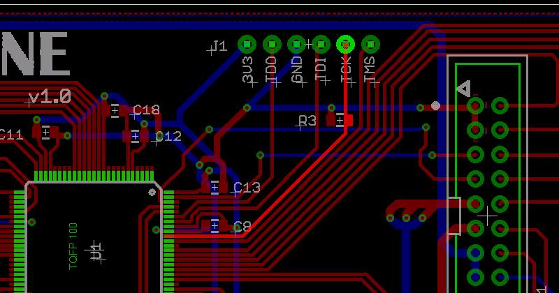
There’s not much opportunity for interference. The only PCB tracks that are crossed by the JTAG signals are voltage supplies and the disk I/O signals, which were unconnected during this test.
The prime suspect is R3, a 4.7K pulldown resistor on TCK. This was recommended by Lattice, as a precaution to prevent spurious TCK pulses causing unwanted JTAG activity when no JTAG programmer is present. Lattice technote TN1208 for the MachXO2 family says on page 12-2 “TCK: Recommended 4.7kOhm pull down.” The other JTAG signals discussed here all have internal pull-ups. 4.7K isn’t much, but maybe the JTAG programmer has an anemic drive strength and is unable to drive TCK fully to 3.3V with the pulldown present? I could try removing R3, but that wouldn’t explain why there are also some runt pulses seen on TMS and TDI. I double-checked to confirm I didn’t accidentally use the wrong value resistor for R3, but no: it’s 4.7K as intended. I also measured the resistance between TCK and GND, to see if there’s some other unintended low-resistance path to GND that’s screwing up everything, but it measured 4.7K exactly.
Read 31 comments and join the conversation31 Comments so far
Leave a reply. For customer support issues, please use the Customer Support link instead of writing comments.


Is it something else on the slot connector interfering with the FPGA? What if you only pull the power from the mac and leave all the other pins disconnected?
No, I don’t think so. The first three graphs show major JTAG signal problems even when the card is outside the Apple II, completely disconnected from the slot.
It looks like there’s some problem with the JTAG programmer. In a breadboard test with no FPGA at all, none of programmer’s output signals rise above 1.99V. This is with the programmer’s VCC input connected to a 3.3V supply, and its outputs not connected to anything except the scope.
I think the programmer is supposed to auto-sense the I/O voltage using the VCC input. So with a 3.3V supply connected, the programmer should be driving the I/Os to 3.3V for highs.
It’s almost as if the JTAG programmer has open collector outputs, so the only reason some of the signals reach 3.3V on the Yellowstone card is that the Yellowstone FPGA has internal pullups on those signals. But that doesn’t really make sense – those outputs should definitely not be open collector. And if they were, TCK would never rise above 0 volts on the Yellowstone card, because of the R3 pulldown resistor on the card.
Another clue: the status light on the FPGA programmer normally glows green when it’s plugged in. When I energize the 3.3V supply connected to the programmer’s VCC input (or power up the Yellowstone card, when testing with the card), the light turns red. Yet JTAG programming succeeds, at least externally from the Apple IIe, even with the red status light.
Is it a clone or authentic programmer? Never used one myself, but looks like the ones I see all over eBay.
It is a clone. Authentic ones cost 10x as much. More notes:
In a breadboard test with a 5V supply, the programmer generates 3.66V outputs. So in both cases, the outputs are about 1.3V below the supply, instead of going all the way to the supply voltage.
I disassembled the JTAG programmer. There’s a 51 ohm series resistor on each output. The outputs are driven from a 74LS244SJ chip, which is powered directly from the VCC input. As an LS series chip, the 74LS244SJ is not supposed to drive rail-to-rail. The 3.66V outputs I observed with a 5V supply are about right on spec, according to the datasheet. Assuming I’m looking at the correct datasheet, the chip isn’t even specced to function with a 3.3V supply (min supply is 4.75V). So this just looks wrong. But maybe my assumptions are wrong – I looked at a generic LS244 datasheet, since I couldn’t identify this one’s manufacturer and I’m not sure what the SJ suffix means (device package variant?)
OK, I’m mostly convinced this is a flaw in the design of this Lattice clone JTAG programmer. Having an LS244 as the output driver just doesn’t make sense. Anybody else agree or disagree? I would welcome some confirmation, before I start ordering replacements.
1. I could buy another of the same Lattice clone programmer, hoping that the LS244 was some kind of one-off production error and not a designed-in flaw. Judging by eBay photos, there’s basically just a single model of Lattice clone programmer, so there’s no real variety available.
2. I could buy a 74LVC244 chip and rework the programmer’s PCB to replace the LS244. That would be interesting, and it might work. But if all the Lattice clones have this same flaw, then future Yellowstone customers will run into the same problem I did if they use clone programmers for JTAG updates. I really need to solve the root problem somehow, if I hope to eventually make this a saleable product and not just a one-of-a-kind curiosity.
3. I could buy the real HW-USBN-2B from Lattice for $162. But again that wouldn’t really solve the problem of how future customers can do JTAG updates without spending a pile of money.
I’d find someone that has one and see if they will open theirs up and compare to yours. Maybe ask on Reddit or a GitHub project that recommends that programmer. There’s also gitter.im/scanlime/live
Maybe try the Adafruit FTDI breakout board. In my experience, it is recognized as a Lattice FTDI programmer (2B type) when plugged in.
https://www.adafruit.com/product/2264
They come into and out of stock on a regular basis, but are generally available.
Or, you can buy a Lattice XO2 Pico board, and remove some resistors to disconnect the JTAG signals from the chip on the board, and instead wire them to a short cable to program another board. It then becomes a general purpose Lattice programmer.
Thanks for the suggestions. There are two needs here – one for me to move forward with development (probably buy the $162 HW-USBN-2B from Lattice) and the other to find an inexpensive and simple (?) Lattice JTAG solution for future Yellowstone owners who want to mod the firmware. There are also two classes of JTAG programmers: ones that clone the Lattice programmer, and work inside the Lattice Diamond software for programming, debugging, etc, and generic JTAG devices that could theoretically do programming with an SVF file and the FPGA’s boundary scan file (I’ve never tried this method). I’ve been focusing on the clone Lattice programmers, of which there seems to be only one kind on eBay, although it has a few different designs on the top plastic.
I would be very surprised if the Adafruit breakout board can function as a Lattice clone inside the Diamond software. You’ve tried it with their software and found it works? That would be great!
Hacking an XO2 Pico board would meet my needs, but is probably a step too far to expect future customers to do this.
I think I’ll focus now on pushing forward my own development, and not worry too much about hypothetical future customers yet. I’ll probably hack my programmer to replace the LS244 with an HC244 and see if that works. I’ll also buy another one of these Lattice clones, to see if this was a one-time error or a systemic design flaw. If it’s systemic, I’ll explore other JTAG programmer options later.
I think I see what may have happened with the LS244SJ. The SJ suffix means it’s a SOP-20 package, with a 12.5mm x 5mm body not including pins, and that’s what the programmer’s PCB is sized to accommodate. But for unknown reasons the SOP-20 package seems to be out of favor, and every ‘244 chip at Digikey is an SSOP or SOIC package. I had to go to eBay to find an HC244 SOP-20 for experimenting. Whoever built these clones probably couldn’t find any source of HC244 chips in SOP-20 package, and scrounged some LS244 chips instead. Looks like they need to do a redesign of their PCB to use a SSOP or SOIC footprint.
Did you buy your programmer recently? If so, I could believe that those chips are hard to find now and they just replaced them with something similar and you might be one of the first people to find out about this incompatibility.
Could be. I bought it last July. One other mystery solved: I mentioned the status LED with the confusing behavior: glows green when the target device is off but turns red when the target is on. This is a tri-color LED in the programmer that was installed backwards. There isn’t any special logic controlling the color – it’s just a straight connection to the two power supplies. If the programmer is powered, you get green. If the target device is powered, you get deep red. If both are powered, you get green+red which looks like an orangey red.
Last comment before I retire this topic: The description for the Lattice clone programmer actually doesn’t say anywhere that it supports JTAG I/O at 3.3V. It’s a clone of the HW-USBN-2A, which does support 3.3V I/O, but maybe this clone was never intended to and I was wrong to assume it did. I found another Lattice clone that looks identical except for a re-branded sticker on top, but this one specifically says “Support JTAG I/O voltage: 1.2V,1.8V,2.5V,3.3V or 5.0V”. I’m crossing my fingers…
Time for a Big Mess O’ Wires JTAG programmer too, maybe?
I am glad that you are working on Yellowstone again. I hope you get the programmer issues solved soon. I wonder if any of the other inexpensive JTAG programmers would work, or if Lattice’s software is specific for theirs? I’ve heard that Xilinx’s software is pretty picky that it is used with an “official” progammer and that Altera’s is less picky, but that’s only what I’ve gathered from googling so I wouldn’t take it as gospel or anything.
Anyway, I hope that you can prove this thing works soon… I’m looking forward to being able to buy one…
https://www.aliexpress.com/item/USB-Download-Cable-Jtag-SPI-Programmer-for-LATTICE-FPGA-CPLD/32597453730.html
I assume at that price those are “counterfeit”… I wonder if they are all the same as the one you got?
Yeah, those $20 ones are all cheap clones. If you look carefully, you’ll see they all have the exact same case, with the same ports and status LED in the same locations, and the only thing that differs is the sticker on top and whatever extra cables they include. So while it may appear there are lots of different people selling clones, in reality it’s lots of different people selling the *same* clone.
I kinda figured that was the case, or something close. I guess if I got one of those just to be able to program an update to a card I wouldn’t mind too much if I had to take the card out of the Apple II in order to do it. Probably easier that way anyway to get the JTAG wires hooked up. Anyway, as I’ve said before, such small issues would not dissuade me at all from wanting one of these cards if you build it. I probably wouldn’t be able to justify buying an “official” Lattice programmer unless I was planning on designing around their FPGAs. While I would never say never, right now I’m leaning towards Altera with Xilinx as a 2nd possibility, although I am not at the point where I’m ready to take that on, I’ve got a few other things I need to learn first. Anyway… $20 for a programmer, even if it doesn’t work or I end up not using it more than once or twice, I’m not out that much.
IIRC you can use an SVF file out of the lattice tools with other JTAG programmers and tools
ex: https://www.sharebrained.com/2012/05/12/debugging-lattice-fpgas-for-the-impatient/
Thanks for that scatterbrained2, it may come in useful. If that works, then probably the $10-$20 JTAG programmers that are available out of China may work.
Here is something interesting I found… a < $10 programmer that claims to work with Lattice FPGAs. https://store.tinyfpga.com/products/tinyfpga-programmer
I’ve seen those tinyfpga boards but didn’t think about the programmer. And being open source, you can even add the components into your project and the user would only need to plug in a USB cable to be able to reprogram it.
I think I’m going to get a tinyFPGA and the programmer… It looks like a nice way to learn FPGA. I’ve been trying to decide between Altera and Xilinx… but this may push me to start on Lattice instead. That hadn’t been something I was considering… but the tinyFPGA is so inexpensive and looks so easy to work with I think I’m sold…
I have a TinyFPGA A1 and the TinyFPGA programmer. Yellowstone uses the same FPGA as the TinyFPGA A2, although in a different package. The TinyFPGA programmer may work as a stand-alone SVF player for Yellowstone, but I haven’t had an opportunity to try it.
That would be a cool thing if it worked, that is a very inexpensive solution to the programming issue.
One thing that I noticed about the inexpensive Lattice programmers on Aliexpress… some of them have labels that are black and white like yours and others have one that is printed in color. I don’t know if there is any significance to that, or whether they are all actually the same inside. Also, while most of them have the beige case that is the same size and same position of status LEDs, there are a few that have a smaller looking black case. Since the case geometry is different I’m guessing there is a chance that what is inside is different, but I could be wrong.
Surgery on the Lattice clone was successful! I used hot air to remove the LS244, replaced it with an HC244, and then wasted 15 minutes trying to debug a circuit that was turned off and unplugged. DOH! Once I remembered to turn on the device power, the modified Lattice clone now succeeds at JTAG programming with the card outside or inside the Apple IIe. The JTAG I/O voltages go nearly all the way up to 3.3V. Now I can return to whatever I was doing before – trying to make this card actually do something useful.
Fantastic! Great reverse engineering and debugging skills there.
Hooray! All this over them saving a few cents on a cheaper part… 🙁 Glad you figured it out.
You can use a Bus Blaster – I do (at work). The FTDI chip is recognized by Diamond Programmer and works fine – you only need modified logic for the level translator CPLD on the bus blaster that keeps the outputs enabled. The stock logic has output enable, which the lattice software does not drive.