Archive for September, 2013
Nibbler Demos!
After fiddling with Nibbler’s hardware and fixing its glitches, it’s time to write some demo software. Let’s see what this little handmade 4-bit CPU can do! Sorry the quality on these videos isn’t the best – try changing the quality setting to 480P to get a bit more picture detail.
Mastermind
Gamers of a certain age will doubtless remember Mastermind, a code-breaking game for two players, which is based on an old pencil and paper game called Bulls and Cows. The codemaker chooses a secret code that’s four elements in length, where each element can be one of six possible colors. The codebreaker then has ten chances to guess the secret code. After each guess, the codemaker gives feedback in the form of black or white pegs: a black peg means some element is the right color and in the right position, and a white peg means some element is the right color but in the wrong position. The feedback pegs are position-independent, so a black peg doesn’t tell the codebreaker which of the four elements in the guess was correct.

Adapting Mastermind to Nibbler was relatively simple. A few weeks ago I wrote a Guess the Number program for testing purposes, and most of it was reusable for Mastermind. The final program was 2057 bytes, or just over half of Nibbler’s available program memory. Instead of using colored pegs, the code is a 4-digit number, where each digit is between 0 and 5. I added a few little bells and whistles, like button feedback sounds, and a little victory tune when you guess the secret code correctly. The result is surprisingly fun, if you like these kinds of logic puzzles. It works fine in the Nibbler simulator too, if you want to try it out.
Blue Danube
I wanted to focus on music and audio next. Nibbler doesn’t have any real audio hardware, only a speaker that’s directly connected to a digital output pin. Making sounds is as simple as toggling the output quickly between 0 and 1, but making specific sounds at just the right frequency is more complicated. It requires a lot of cycle counting math, to guarantee the speaker will be toggled at exactly the right rate for an A at 440 Hz or a piano’s middle C (261.6 Hz). Each period of the waveform needs to be exactly the same length, even as the path through the inner code loop varies in length due to carry propagation with multi-nibble counters. If one period is slightly off, your ear will hear it.
Setting the duration of each note involves more math, dividing the duration by the period length to find the number of periods to play. That means two notes at different frequencies but with the same duration will have different repeat counts (duration values) in the code, further adding to the necessary bookkeeping.
I started writing a music demo by hand, but it was such a pain that I couldn’t imagine building a whole song that way. Instead, I created a new tool called Music Maker to do the math and code creation for me. It takes song data as input, and generates a Nibbler assembly program as output. The song data is expressed in the Music Macro Language from Microsoft Basic, which you might recall if you ever used GWBASIC’s PLAY command. This simple one-voice text-based format is a perfect match for Nibbler’s limited audio capabilities. Songs are described as a series of notes, with optional length and octave modifiers:
"T180 DF#A L2 A L4 O4 AA P4 F#F# P4 O3 D"
Music Maker saved me a huge amount of effort, but I still needed to hand-edit the generated assembly code to repeat a few musical phrases in the right spots. Because Nibbler’s instruction set isn’t well-suited to storing constant data in programs, the code is fairly bloated, taking 3569 bytes (87% of memory) for a song that’s a few dozen measures long. I chose the Blue Danube for the demo song.
Frogger
For the last demo I wanted to do something really different, so I created a real-time action game using custom graphics. The classic arcade game Frogger leapt to mind. The player must guide a frog across many lanes of traffic and a treacherous river, avoiding a variety of obstacles moving in different directions and at different speeds.

Bringing Frogger to Nibbler presented several challenges. First – graphics. The HD44780 chip inside the 16×2 character LCD screen does support user-defined character fonts, but only for eight characters, which doesn’t provide a lot of variety. Second – screen size. The screen only has two rows, and that’s not many lanes of traffic for our frog to dodge. How can you make a game with that?
Each character on the LCD screen is 5×8 pixels, so the total screen height is 16 pixels. My approach was to divide the screen into four virtual rows, each of which was 4 pixels tall, with two virtual rows per actual row of text characters. Then I created custom character fonts for each possible combination of contents in the cells in the upper and lower virtual rows. Each cell can contain one of three possible items (an obstacle, the frog, or nothing), and there are two cells, so there would seem to be 3×3 or 9 permutations. But because there’s only one frog in the game, the permutation with frogs in both cells isn’t needed, and the remaining eight permutations fit exactly into the HD44780’s eight user-defined character slots. The result is a 16×4 virtual playfield, where each playfield cell is 5×4 pixels. For a bit of added variety, I also made the upper and lower obstacles look visually distinct.

To make the game “real-time”, I needed a way to animate the obstacles while the player was moving. Without interrupts or any other real time-keeping mechanism, I had to add a timeout counter inside the busy loop that checks for button input. After a few thousand checks of the button state, the game jumps to a routine that moves the lanes of obstacles by one position, then returns to button checking. Fortunately it all happens fast enough that you can’t notice any hiccups.
Frogger was the only demo where the lack of an indirect addressing mode really hurt. Tasks like animating the playfield or checking for collisions are just screaming out for indirect addressing. Without it, I had to write code that explicitly copies/checks/moves each of the 64 playfield cells. The result is lots of ugly bloat, and a code size of 3279 bytes (80% of memory).
The final game turned out nicely! The only big flaw is the animation: the persistency of the LCD screen makes objects appear to fade and flicker, but there’s nothing I can do about that. Despite this, it’s a lot of fun to play. In the video, notice that the lanes of obstacles animate at different speeds, and each lane moves in the opposite direction from its neighbors, making the game more challenging than it first appears. If you can navigate the frog upwards from the bottom row, and escape out the top row, you’ll hear a little victory tune. Go Nibbler!
Read 5 comments and join the conversationEntry-Level Oscilloscopes
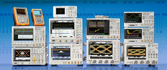
It’s time to shop for a new oscilloscope. My trusty HP1631d has served me well, but it’s almost 30 years old, and it’s not even really an oscilloscope but a logic analyzer. This boat anchor is big, heavy, loud, cumbersome, and feature-starved. I’ll probably still keep it around for the logic analyzer functions, but for traditional oscilloscope work I’d like something more modern.
Fortunately, this is a great time to be a hobbyist looking for a low-cost scope. There’s practically a tidal wave of entry-level digital scopes coming out of China today, with plenty of good options in the $300-$400 range. The only problem is there are so many options, it can be hard to sift through the blizzard of information and specs in order to choose one!
Why a new entry-level scope, instead of a used digital or analog scope from somebody like Tektronix, which might be purchased for the same price or less? There are some great values on eBay and Craigslist for sure, and for someone on a minimal budget, I think an older used scope is the best option for getting started in electronics. But the major drawback of all those used scopes is that they’re invariably big, heavy, loud boat anchors. They also lack modern connectivity options like USB. I’ve already got a boat anchor, thank you.
When shopping for a scope, there are three primary specs that get the most attention: bandwidth, sample rate, and memory depth. I had only a hazy understanding of how these were related until I began studying a few days ago.
Bandwidth
Bandwidth determines the fastest signal you can measure with the scope. It’s determined by the scope’s front-end electronics, as well as by the probes you’re using. But does that mean a 50 MHz scope is good for measuring signals up to 50 MHz, and useless for anything beyond that? No. The definition of bandwidth for oscilloscopes is actually very specific: it’s the frequency at which the measured amplitude of the input signal is decreased by -3dB (about 30%) of its original value. If you view a 50 MHz sine wave that’s 1v peak-to-peak on a 50 MHz scope, the scope will show 0.7v peak-to-peak. You can view signals faster than 50 MHz on the scope, but they’ll be attenuated even more than -3db. Signals slower than 50 MHz will be attenuated too, but by less than -3db. There’s no magic cutoff at 50 MHz where the scope just stops working.
Sometimes you’ll also see a scope’s rise time advertised. This is the time the scope requires to move from 10% to 90% of a new voltage input. By doing some math, you can demonstrate that bandwidth in GHz is approximately 0.35 / rise time in nanoseconds. So a scope with a 7 ns rise time should have a bandwidth of 0.35 / 7 = 0.05 GHz = 50 MHz.
OK, a little attenuation doesn’t sound so bad. But typically you won’t be measuring sine waves, you’ll be measuring things like square waves. You probably know that square waves are composed of an infinite series of sine waves at odd harmonics of the fundamental frequency. A 40 MHz square wave can be thought of as a 40 MHz sine wave, plus 1/3 of a 120 MHz sine wave, plus 1/5 of a 200 MHz sine wave, plus 1/7 of a 280 MHz sine wave, etc.
If you view that 40 MHz square wave on a 50 MHz scope, it can see the 40 MHz fundamental sine wave, but all the harmonics are above its bandwidth, and are attenuated into insignificance. The result is that the 40 MHz square wave looks like a 40 MHz sine wave when viewed on the 50 MHz scope. That’s really bad. If all you care about is knowing the signal’s frequency, then I guess it’s OK, but the actual shape of the signal is completely lost. If you want to measure the signal’s rise time or duty cycle, you just can’t do it on that scope.
This explains why you need a scope whose bandwidth isn’t just strictly higher than the frequency of the fastest signal you’ll be measuring, but much higher. How much? A common rule of thumb is 4x-5x higher. At 5x, the first two harmonics of the square wave will fall within the scope’s bandwidth, so that seems like a good place to draw the line. But really I think this is one of those “it depends” situations. If almost all the work you do is at 10 MHz or below, but you occasionally have some elements that run as fast as 30 MHz, then you’ll probably be fine with a 50 MHz scope. It just means that when you do need to examine a 30 MHz signal, it will be as if looking through a clouded glass, where the true shape and amplitude of the signal are partly obscured. If you just need to know whether there’s any signal at all, or what its frequency is, then that’s fine. But if you need to look for small glitches or timing problems at 30 MHz, it may not be.
Sampling Rate
All modern oscilloscopes are digital, and sample the input signals millions or billions of times per second. But how fast does the sampling rate need to be, and what’s its relationship to the bandwidth? When I first began looking into it, I thought sampling rate only needed to be 2x bandwidth (Nyquist). While that’s enough to reconstruct the input signal’s frequency, it won’t tell you anything about its shape. At 2x, you’ll get one sample during the high part of each period, and one sample during the low, but you’ll have no idea if the signal is a sine or a square or a lumpy shape. The common rule of thumb is that the sampling rate should be 4x-5x the bandwidth. So if you typically need to examine 20 MHz signals, you should look for a scope with 100 MHz bandwidth and 500M samples/sec.
On most scopes, the sampling rate is cut in half when using two channels instead of one.
Memory
All those digital samples have to be stored somewhere. With more memory, the scope can store more of them. The obvious result of having more memory is that the scope can capture a longer time duration in a single acquisition, which can be useful if you need to debug something like a lengthy serial communication. Or it can store more samples during the same time duration, making it possible to zoom in on the acquired waveform to examine small details.
Not all oscilloscope memory is created equal. Many scopes have standard memory and “long memory”, which operate at different speeds. The long memory stores more samples, but can’t store them as fast as standard memory, so the sampling rate must be reduced when long memory is used. Other scopes have long memory that operates at full speed. This is an important consideration that’s generally not mentioned anywhere in the scope’s advertised specs, but must be inferred from careful reading of the manual or datasheet.
Bandwidth + Sampling Rate + Memory = Confusion
It’s important to recognize that a scope’s advertised sampling rate is its maximum sampling rate, but the actual sampling rate may be much lower. As described above, the use of two channels or slower “long memory” are some reasons that the sampling rate may be reduced below the maximum. But the main reason is that the rate must be reduced when the capture duration increases, in order to keep the total number of sample points small enough to fit in memory. For example, if you want a 50 microsecond per division timescale, that’s a 500 microsecond capture duration. If your scope has 10K points memory, you can only sample the signal at 10000 / 500 us = 20M samples/sec, regardless of how fast the scope’s maximum sample rate is.
When the scope’s sample rate is reduced, its effective bandwidth is also reduced. At 20M samples/sec, the scope has no hope of capturing signals faster than 10 MHz, and won’t be able to faithfully capture the shape of signals faster than about 2 or 2.5 MHz. This leads to the conclusion that memory size constrains bandwidth. That may be old news to some, or a total surprise, as it was for me. With a small memory, at longer timescales, a fancy 200 MHz scope may essentially turn into a 10 MHz scope.
Examples in the Real World
Take a look at this table, which I found on an oscilloscope forum. It compares two popular entry-level oscilloscopes with 100 MHz bandwidth and 1Gs/sec sample rate: the Rigol DS1102e, and the Owon SDS7102. The specs are the same, so you might expect they would have the same basic capabilities for signal capture, but that’s not true. The Owon has 10M points memory per channel, while the Rigol has 1M points shared between both channels. The Owon memory also runs at full speed, while the Rigol’s long memory runs at half speed. The red line shows the point as which the effective bandwidth is reduced below 100 MHz.

The result of 20x more memory and 2x faster memory is a big performance advantage for the Owon. In dual channel mode using the full memory capacity, the Owon can do 500Ms/sec while the Rigol can only do 250Ms/sec. At longer timescales, the difference grows larger. At 1ms/division, the Owon can still do 500Ms/sec while the Rigol is slowed to only 20Ms/sec – a 25x difference! You would never know this if you only looked at the advertised bandwidth and sample rate figures from the manufacturers.
Does this mean the Owon is a 25x better scope than the Rigol? Definitely not. For one thing, most reviewers seem to feel the Owon’s UI design is somewhat clunky and confusing compared to the Rigol. But even looking just at measurement capabilities, you could definitely argue that capturing at 1ms/division while retaining 100MHz bandwidth isn’t very useful in the real world. Most of the time, if you want to examine high speed signals in the greatest detail, you’ll capture them with a short timescale like 50ns, where the sample rate difference between the two scopes is only 2x. And if you’re just looking at a single edge or small number of signal periods, then you won’t need the Rigol’s long memory, and there won’t be any sample rate difference at all.
Bandwidth Hacking
One wrinkle that complicates the shopping process is that some scopes from Rigol and Hantek can be “hacked” in software to unlock higher bandwidths. I first read about these hacks a couple of years ago, but thought they were bullshit. Sure, you might unlock the menu options for higher bandwidths, but if the scope’s ADC and other front-end components only had 60 MHz bandwidth, there’s no way a software change could magically make it into a 200 MHz scope. But after doing much more research, it seems that all scopes in Rigol’s DS1000 line and Hantek’s DSO5000 line are actually 200 MHz scopes, with some models crippled in firmware to limit their bandwidth. People smarter than me have done bandwidth measurements on the hacked scopes, and even disassembled 200 MHz and 60 MHz scopes from the same family. They proved that the internal electronics are the same, and a 60 MHz scope hacked to 200 MHz really does have 200 MHz bandwidth.
Assuming such hacks really work, are they ethical? Are they like pirating software (which I don’t), or more like unlocking your CPU multiplier so you can overclock it (which I do)? Or like jailbreaking your iPhone? My moral compass doesn’t have any problem with it, but I’ll reserve the right to change my mind.
The Contenders
After staring at various oscilloscopes until I was blurry-eyed, I’ve narrowed the list of contenders to just a few.
Rigol DS1052e / DS1102e – This scope has been around for several years now, and has a pretty good reputation. The 50 MHz version can be had for about $300, and can be hacked to 100 MHz. I even used one of these at work for a while. But the DS1000 line is getting a bit old and crufty, with a smaller screen and fewer features than some of the newer competition. I’ve more-or-less ruled it out.
Owon SDS7102 – The Owon has the largest, fastest memory of any entry-level scope today, with 10M points per channel full-speed memory. It also has a very nice 800 x 600 8″ display. It can be purchased for about $420 including shipping, and reviewers on Amazon.com give it an average rating of 4.5 stars. I was very excited about this scope initially, but reviews on electronics web sites haven’t been as enthusiastic as Amazon’s. Many people complain about the user controls being somewhat clunky and confusing. It sounds like the interface isn’t terrible, just kind of annoying. Is it worth being annoyed by your scope every time you use it, in exchange for better sample rates or longer captures in the rare cases when you need them? Probably not.
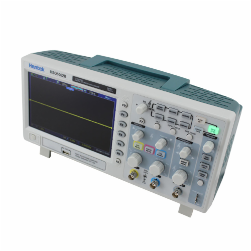
Hantek DSO5102B – This same 100 MHz scope is also sold under several other brand names and model numbers. There’s an epic 2000 post discussion thread about this scope on the EEVblog forums, describing how to hack it to 200 MHz, modify the interface screens, and tweak other features. Even unmodified, it seems to be a fairly popular and easy to use scope, with most people scoring it best among the entry-level scopes for user interface and features. It’s about $370 including shipping. This is my leading choice at the moment. I was almost ready to buy it before I watched Dave Jones’ video review of it on EEVBlog, where he initially seemed quite pleased with it before he ran into some problems, and finally gave it a thumbs down.
Hantek DSO5062B – This is the 60 MHz version of the Hantek line, and sells for about $345 shipped – $25 less than the 100 MHz model. Both can be hacked to 200 MHz. 100 MHz is really plenty for me, so is it worth $25 to avoid the hassle of hacking the 60 MHz version, and any possible problems it might cause? Yeah, I think it is, so the DSO5062B is probably out of the running.
Hantek DSO5102P – This is the 100 MHz model, but without long memory. It’s $320 shipped, or $50 less. How useful is that long memory, really? There’s no question it could be useful in some situations, but most of the time I’m guessing I wouldn’t use the long memory at all. Why pay for a feature you’re not going to use? Saving $50 sounds good, but when I run into a situation where the long memory would have been useful, I’ll probably wish I hadn’t been so cheap.
Hantek DSO5072P – This scope is 70 MHz, without long memory, but otherwise the same as the other Hanteks. It too can be hacked to 200 MHz, and it’s only $270 shipped. That’s $100 cheaper than the DSO5102B. For $100, would I go through the headache of hacking the scope, and give up the long memory? Hmmm, maybe.

Rigol DS2072 – This last scope is really in a different class than all the others. The major specs are about the same, but the build quality, features, and overall polish are much higher than the others. Dave Jones made an EEVBlog review where he positively gushed about this scope. The only problem is that it’s $840, and that’s for the 70 MHz version! The 100 MHz version is a smooth $1143. But like the other Rigols, the 70 MHz model can be hacked to 200 MHz.
What do you get for $840 vs $350 or so for the other scopes? For starters, the sample rate is 2Gs/sec, as opposed to 1Gs/sec on all the other scopes I mentioned. Long memory is 14 million points, expandable to 56 million. Jitter, noise floor, and all those other details are much better than with the other scopes. It’s a so-called DPO (digital phosphor oscilloscope), where many copies of a periodic waveform are overlaid onscreen with an intensity gradient that’s similar to an analog scope display. Its waveform refresh rate is extremely high, at around 40,000 waves/second, making it great for catching rare glitches. It always runs the sampler at the maximum sample rate, doing averaging on-the-fly when necessary to keep the number of stored samples small enough to fit in memory. It has some very, very cool waveform analysis features. And it even has some basic logic analyzer functions, like automatic decoding of SPI and I2C traffic.
If Santa Claus were bringing me a free oscilloscope, I’d ask for the Rigol DS2072. But if I’m paying out of my own pocket, I’m not convinced all those nice features justify a 2.5x price difference. At the end of the day, I’ll still be looking at the same basic signal on either scope. Bells and whistles are great, but maybe not 2.5x great.
Your Toyota vs. my Horse
Shopping for a new entry-level scope to replace my HP1631d has been funny at times. Even the worst of the contenders are still miles ahead of the 1631d in most respects. It’s amusing to read complaints about scopes that “only” refresh 40 waveforms/sec, when my current scope can barely manage 2 waveforms/sec. Or to read discussions about whether the Hantek –P models are hamstrung by having “only” 40K points of sample memory, when my current scope has just 1K points. 1K!
Read 22 comments and join the conversation
Invalid Logic Levels Explained
What happens when you feed an invalid voltage level to the input of a digital logic gate? It’s an interesting story. In my last post, I described a subtle Nibbler bug where a combinatorial feedback loop through the ALU caused an invalid voltage level to propagate from an output back to the input, creating a self-sustaining cycle of badness. I fixed the problem by adding another chip to break the loop, but I wasn’t totally happy with that solution. After studying the problem further, and peering into the internal details of the 74LS181 ALU chip, I’ve found a new solution that doesn’t require any extra hardware. The new chip has been removed, and Nibbler still runs flawlessly.
To explain what’s going on, it’s important to understand how basic logic gates like NOR and AND are built from transistors. The diagrams below show gates using FET transistors, instead of the bipolar transistors used in the 7400LS family, but the concept is the same.

In the NOR gate, if either A or B is above the transistor switching threshold, one or both of the bottom transistors will be turned on. This pulls the output to ground. The top transistors will be turned off. If neither A nor B is above the switching threshold, neither of the bottom transistors will be turned on, but both of the top transistors will be on, pulling the output to Vcc.
In the AND gate, the top and bottom portions are reversed, and an inverter is placed at the output of the first stage to create an AND instead of a NAND.
Now let’s assume B is at an invalid voltage level, right around the transistor switching threshold, while A is zero volts. In the NOR gate, one of the bottom transistors will be off, and the other will midway between off and on, acting similar to a resistor. One of the top transistors will be fully on, and the other will be midway between off and on. The result is that both the top and bottom sections will be partly on, creating a path from Vcc to ground, and resulting in an output voltage that’s somewhere in the middle.
If B was invalid while A was at Vcc, then one of the bottom transistors would be fully on, and it wouldn’t matter that the other bottom transistor was midway between off and on. Similarly, one of the top transistors would be fully off, so the other transistor wouldn’t matter. The output would be 0 volts regardless of the voltage at B.
Applying the same reasoning to the AND gate, these rules emerge:
- ? NOR 0 = ?
- ? NOR 1 = 0
- ? AND 0 = 0
- ? AND 1 = ?
Now let’s apply these rules to a section of the 74LS181 internal logic, taken from its datasheet. In the case where Nibbler was failing, the ALU function input S was all 1’s, the A input was also all 1’s, and the B input was momentarily at an invalid voltage level. The blue numbers show the propagation of values through the first input stage of the ALU.
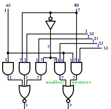
In this case where S is all 1’s, the ALU output is supposed to be A, and the B input shouldn’t matter. And logically, that’s what happens. The three gates on the right compute the expression A0*/B0*S2 NOR A0*B0*S3, which here reduces to /B0 NOR B0, which is always 0 regardless of the value of B0. So B is irrelevant. But electrically it’s a different story. The ? values propagate through the gates. ? NOR ? is not 0. The ALU outputs ? values to the data bus, which eventually propagate back to its B input, continuing the vicious cycle. The circuit doesn’t work.
But wait! On the ‘181 ALU, there are actually two different ways to output the value of A. I arbitrarily chose one of them when I designed the microcode. The other way sets the ALU function input S to all 0’s instead of all 1’s. What happens in that case?
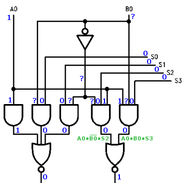
The ? values are stopped dead at the first input stage, and don’t propagate any further into the ALU. The circuit works.
Applying this to Nibbler was easy. I just changed the microcode to use the 0000 output function instead of the 1111 function, and removed the extra chip that I previously added to break the feedback loop. Happy times!
Read 2 comments and join the conversationSneaky Combinatorial Feedback Bugs
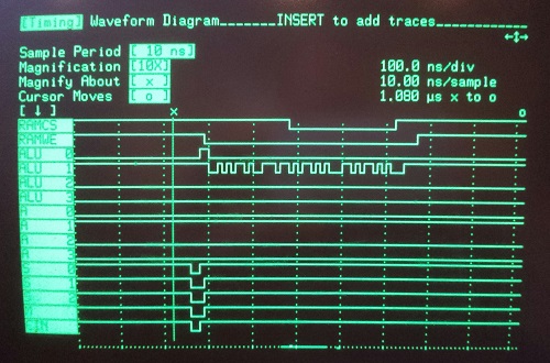
Aha! After four days of tinkering with Nibbler, I finally found the cause of the occasional bad writes to RAM. At first I thought it was a timing problem with the RAM enable signals, then I thought it was bus contention, but the key piece of evidence was the logic analyzer trace you see above. The X cursor marks the start of a clock cycle. The CPU is attempting to take the number 2 in the accumulator, pass it through the ALU, and write it to RAM. Shortly after the start of the clock cycle, you can see that the ALU function inputs glitch briefly. After that, the ALU outputs all adopt the same values as the accumulator, except for ALU1, which demonstrates some crazy noise. This only happens rarely – maybe one in ten thousand writes to RAM – but when it happens the wrong value gets stored.
What could cause that horrible-looking signal on ALU1? The ALU is just passing through the value of A, and A looks fine, as do the ALU function inputs S, M, and Cin. The sneaky answer is that the problem is caused by the ALU’s B input, which isn’t even being used during this operation.
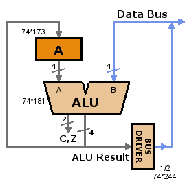

The diagram on the left shows the problem. When the ALU bus driver is enabled, the ALU result value is driven onto the data bus, where it makes its way back to the ALU’s B input. I thought this was OK, as long as the ALU function was set to something that only used the A input, and was independent of B. From a logical standpoint, that’s true, but from an electrical standpoint it’s not. Even though the value at the B input is logically irrelevant, if an invalid voltage around 2.5v appears at the B input, it will result in an invalid voltage at the ALU output. The bus driver has the same logic thresholds, so it also sees an invalid input voltage and produces an invalid output voltage, which appears back at the ALU’s B input, completing the feedback cycle. Garbage in, garbage out.
This should be a rare occurrence, and it is. Any little noise or voltage drift that pushes the bus to a valid 0 or 1 voltage will break the cycle. My suspicion is that in some circumstances, the internal structure of the ALU (a 74LS181) is such that a negative feedback loop is created on one of the bus lines. If the bus line voltage drifts up by epsilon, the ALU will output a voltage that’s lower by epsilon, which will be reflected at the bus driver output, counteracting the drift. It would be similar to connecting the output of an inverter to its input.
My solution is shown in the diagram on the right. A 74HCT157 two-input multiplexer was added to the ALU’s B input. Normally it passes the data bus value through to the B input, but when the ALU drives its result onto the bus, the mux passes zero to the B input instead. It doesn’t really matter what value is passed to the B input, as long as it’s something valid.
At first I was reluctant to call this “the cause of the problem”, because I’ve been through so many other apparent solutions in the past few days. At one point I thought that adding capacitors to the data bus fixed the problem, then replacing the bus driver HCT chip with an LS chip, or the fetch register. But none of those solutions actually explained why things didn’t work originally, nor why they fixed the problem. And after more careful testing, replacing the bus driver or fetch register with LS-family chips didn’t actually fix the problem 100% of the time. The combinatorial loop is the only scenario that explains why things weren’t working originally, and that works 100% reliably in all the tests I’ve made after adding the mux.
I’m happy to have finally found the answer to this mystery, but a little unhappy with the form the solution takes. Looking at the revised architecture diagram, it’s not at all obvious to the casual observer why there should be a mux there. The fact that it’s required for electrical reasons and not logical reasons is even worse. It just doesn’t feel “clean”, in some hard to define way. Perhaps there’s a better solution, but at this point I’ve spent so much time trying to fix hardware this problem, I just want to move on to writing more fun Nibbler software now.
Read 18 comments and join the conversation
De-Glitching RAM Writes
Yesterday’s Nibbler celebration was premature – I discovered that about one in ten-thousand writes to RAM stores the wrong value. Bad RAM, bad! No biscuit for you!
Arghh, what a headache. I first discovered the problem while making improvements to the guess-the-number game. After many experiments, I was able to boil it down to a case where $F is written to RAM, but something else is read back. And I proved that it’s the write operation that’s going bad, not the following read. But that’s about as far as I’ve gotten in understanding why it fails, or how to fix it.
    ; Example 1 - fails consistently
    #define TEST_LOCATION $038

    testram:
        lit #0
        addi #15
        st TEST_LOCATION
        ld TEST_LOCATION
        cmpi #15
        jz testram

    fail:
        ; turn on the debug LED
Example 1 adds 15 to 0, stores the result, reads it back, and checks to make sure it’s 15. If not, it turns on the debug LED to indicate a failure. This test fails consistently, after anywhere from zero to 10 seconds of operation.
    ; Example 2 - works reliably
    #define TEST_LOCATION $038

    testram:
        lit #15
        addi #0
        st TEST_LOCATION
        ld TEST_LOCATION
        cmpi #15
        jz testram

    fail:
        ; turn on the debug LED
Example 2 is identical to example 1, but it adds 0 to 15 instead of 15 to 0. This test works reliably. How can that be? After all, in both examples the entire CPU is in the exact same state at the time of the store instruction. Wait, maybe it’s not the store that’s going wrong at all! Maybe the addi is faulty and computing the wrong sum?
    ; Example 3 - works reliably
    #define TEST_LOCATION $038

    testram:
        lit #0
        addi #15
        cmpi #15
        jz testram

    fail:
        ; turn on the debug LED
Nope. Removing the store/load from example 1, which failed consistently, now works reliably. Head, meet wall. Bang, bang, bang.
Timing
Click on the simplified schematic at the top of this post to see what’s involved while the accumulator value is being written to RAM.
My best guess is that at the end of a RAM write, either the data or the address are changing before the RAM /CS is de-asserted. /CS comes from a 74LS32 OR gate with a max propagation delay of 22 ns. The clock is one of the OR inputs, so /CS will be de-asserted no more than 22 ns after the rising edge of the clock. Could the RAM data or address be changing during this window?
Address: The high address bits come from the Fetch register, whose value never changes at the same time as a RAM write. The low address bits come from the program ROM, which has a 150 ns propagation delay, on top of the PC regsiter’s 39 ns tcq delay, so it seems very unlikely those values could change within 22 ns of a clock edge.
Data: The data is a little more complicated. The value coming from the accumulator won’t change, but the ALU function might, or bus driver B might become disabled, or something else might start driving the data bus and cause contention. All of those would require changing control signals in order to happen. Control signals come from the microcode ROMs, which have a 150 ns propagation delay, on top of tcq delays of about 30 ns for the registers at their inputs. So it seems unlikely the data values could be changing within 22 ns of a clock edge either.
A few other things I tried:
- Replaced the 74HCT244 bus driver with a 74LS244 – This helped a lot, but didn’t completely eliminate the problem.
- Changed TEST_LOCATION to $000 – The test still failed intermittently, but not as much as before
- Changed TEST_LOCATION to $FFF – The test passed reliably
I’m not even 100% certain that the problem is with address or data becoming invalid before the /CS de-assert. Maybe address isn’t valid before the /CS assert, or maybe there’s a glitch on /CS or /WE at some other time. But I don’t think so.
What I really need to do is hook up an oscilloscope or logic analyzer, and look at the relative timing of the clock, /CS, data, and address to see what’s going on. Unfortunately I only have one working scope probe, and even if I had more, I’m not sure the scope has enough resolution to see a timing error of a few nanoseconds. And even if I can demonstrate that data or address are changing before /CS de-assert, I’m not sure what I could do to fix it without major changes. Hmmmm…
Read 27 comments and join the conversationHomemade CPU First Boot

YES, IT WORKS! The Nibbler homemade CPU is up and running, and it can play “guess the number” like nobody’s business. Awesome! If you haven’t seen my earlier posts, Nibbler is a 4 bit CPU built from standard 7400 series logic chips – individual counters, registers, buffers, and gates. It’s an educational example of a simple CPU that’s easy to understand and build, but still capable of running games and other interesting programs. The CPU contains 17 chips in total.
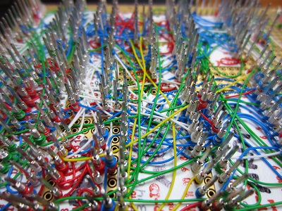
With all the advance design work and simulation that went into Nibbler, I was fairly confident it would work, but it’s sure nice to see it confirmed in real hardware. Construction was slow and tedious, but went fairly smoothly. After soldering the buttons and passive components, the chips were mounted in sockets and connected by wire-wrap. The whole construction process took about five days.
Some specs:
- 4 bit custom-made CPU
- 12 bit addressing, 4K address space size
- Harvard architecture – separate program and data memory spaces
- 2 MHz clock speed, 2 clocks per instruction = 1 million instructions/sec
- Thirteen 7400-series chips in the CPU data and control paths
- Two 28C16 EEPROMs store microcode for generating internal control signals
- 4K x 4 SRAM (CY7C168A)
- 28C64 EEPROM stores programs
- Four pushbutton inputs
- 16 x 2 character LCD
- Audio speaker
- About 100 mA current draw at 5V
For lots more detail on how Nibbler works, see the project home page.
Fun with Debugging
During construction, I ran into a couple of errors in my schematic. I accidentally reversed the Zero and Carry inputs to the microcode ROMs. You’d think that would be an easy thing to catch – notice that all the instructions involving the Carry flag didn’t work, double-check the wiring, and aha! Unfortunately it didn’t happen that way at all.
At the time I ran into this problem, I was part-way through construction, and I hadn’t yet connected the Flags register’s Zero input to anything. It was just floating. Because of my schematic mistake, the CPU was actually using this undefined Zero flag when it thought it was using the Carry flag. The crazy thing was that it still worked sometimes! After powering on the CPU, the Carry flag appeared to work normally and programs ran fine for about two seconds, after which the whole thing went to hell. Because it worked briefly, I assumed there was some kind of overheating problem, or maybe a timing problem caused by changing propagation delays as the chips warmed up. I spent almost a whole day trying to track down the problem. At least it gave me an excuse to use my logic analyzer!

Debugging the Carry flag with the logic analyzer
How is it possible that the CPU worked for a few seconds, when it was using the completely wrong flag? It turns out that because Zero wasn’t yet connected to anything, and the Zero and Carry wires ran side-by-side, capacitive coupling caused the floating Zero input to follow the value of the Carry flag, at least for a little while. What?! Yup, the combination of reversed wires and an unconnected input caused the right value to jump to the wrong wire. After a few seconds, some stray capacitance somewhere charged up to the point where this little trick no longer worked, and the CPU conked out. As soon as I swapped the wires and connected the Zero input properly, the CPU began working nicely.
Son of BMOW 1
It’s interesting to compare Nibbler with BMOW 1, my first homemade CPU. Compared with BMOW 1, Nibbler is tiny! The whole thing fits in the palm of my hand. BMOW 1 looks like a giant in comparison. And Nibbler has just 17 chips, all of which are either memory or 7400 series logic. BMOW 1 has 65 chips, many of which are GALs (programmable logic). The size discrepancy would be even greater if BMOW 1 were constrained to use only 7400 series logic.
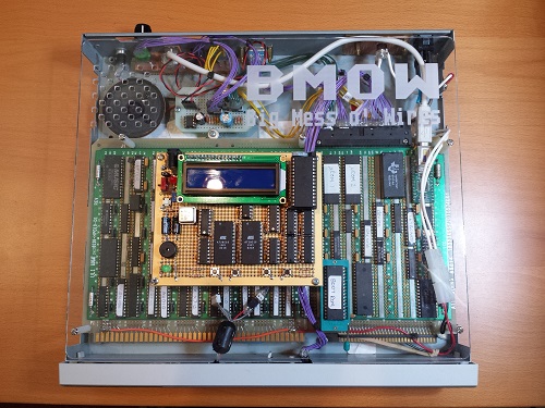
How can Nibbler be that much smaller? The major difference is that BMOW 1 supports lots of I/O devices that Nibbler doesn’t, like a PS/2 keyboard, VGA video, a serial port, 3-voice audio, and a real-time clock. All those device support chips really add up. BMOW 1 also has wider data and address paths, and has a hardware stack register and some other CPU features that Nibbler lacks. BMOW 1 is a very cool machine, but it carries a lot of bloat, making it difficult for people to understand how it all works. Nibbler is more like a minimal CPU example, with just enough power for a few basic games and demos.
Wires!
Because this is the “Big Mess o’ Wires” blog, I’ll conclude with some gratuitous wiring photos. Enjoy!


Read 12 comments and join the conversation


