

Archive for May, 2010
Circuit Board Test
I’ve decided to make a simpler prototype board before advancing to the final Tiny CPU system boards. This will give me a chance to get more familiar with using Eagle, create a circuit board, get it manufactured, and verify that it works. I’m sure I’ll make plenty of mistakes, and the prototype board may not even work at all, but by starting with a non-critical prototype the cost of failure is minimized.
To that end, I spent some quality time with Eagle over the weekend, creating a nine square inch board with a single Altera Max 7128S (in PLCC socket), JTAG header, keyboard connector, LCD header, and some switches and LCDs. It’s much of what I expect to be in the final Tiny CPU system boards, but it lacks the second 7128S needed for device interfacing, as well as RAM and ROM.
Click the images below to see full sized versions, or get the Eagle schematic and board files.


Board Design
To save space and a bit of complexity, there’s no voltage regulator on the board. I plan to use the same 5V regulated power supply that I did with BMOW. VCC and GND are isolated from the DC jack by jumpers, so I can easily measure the board’s current draw, or bypass the DC jack to connect a separate regulated power source.
There are 13 capacitors on the board. Yikes! I followed Altera’s recommendation, and put a 0.01uF capacitor between every power/ground pin pair on the CPLD, eight in all. Then for good measure I also added two higher-valued capacitors, 1uF and 47uF, as well as a 470uF power filter capacitor. The keyboard and JTAG ports both have 0.1uF capacitors across their power/ground pins too. I’m not sure if this many capacitors are really necessary. It was a bit of a pain to deal with them all, and they eat up some board space.
Routing the board was kind of fun, at least for a while. I’d never done anything like this before. I began by placing the components on the board so that related components were near each other, minimizing the length of air wires as displayed by Eagle. I then hand-routed the power and ground busses, using wide 50 mil traces. The power bus is on the top layer, and ground on the bottom. I routed the clock line using a 24 mil trace. The rest of the signal traces are 10 mil. I routed many of them by hand, but eventually I got bored and hit the auto-route button.
I had to guess how densely to space the components when I placed them, and I think I guessed about right. It might be possible to pack everything in slightly tighter, but not much.
Ground Plane
After I was finished, I added a ground plane to the bottom layer. Any empty area that was adjacent to a ground trace got completely filled with copper. As you can see, there are many spots around the edges that the ground plane didn’t reach. I’m unsure if it’s worth adding a few vias to bring ground out to these areas too, or if it’s not a big deal. I could added a ground plane to the empty regions on the top layer too, but again I don’t know if that would help anything.
A Pain in the TQFP
The original design for the board was substantially more complicated, and included a second Max 7128S in a TQFP package with 0.5 mm pin spacing. If I could use that package successfully instead of the PLCC package, it would save a ton of board space. I keep hearing that it’s possible to hand-solder those fine-pitch SMD packages, so I designed the board so that the second 7128S could be added or removed from the JTAG chain with a few jumpers. If I totally botched it and destroyed the chip or shorted some traces, I expected I could set the jumpers to disable it, and still use the first 7128S.
It did not go well. Using the Altera 7128S TQFP100 footprint included with Eagle, the footprint failed the design rule check. The pads only have about 6 mil spacing between them, but BatchPCB’s minimal is 8 mils. I spent quite a long time getting familiar with the footprint editor, and designed a new TQFP footprint with smaller pads and wider spacing that passed the DRC. Unfortunately it proved to be quite a challenge to route. With such finely-spaced pins, it’s not possible to pass a signal trace between pins. And because it’s an SMD part and not-through hole, all signal traces must meet the pin in the top layer, instead of having a choice of top of bottom. It was starting to look as though I’d need board space equivalent to the PLCC package, just to fit the maze of snaking traces and vias needed for the TQFP package. Eventually I tried the auto-router on it, but it fared no better than my manual efforts: we both failed. Ultimately, I gave up and deleted the second 7128S from the design.
Feedback?
Since I’ve never done this before, I’d happily accept suggestions and advice on how this design and board layout could be improved. Leave a comment, or send me an email. See any flaws, potential problems, or just not-so-good techniques? I’m listening.
I’ve uploaded this board to BatchPCB, and it passed their design rule check. The cost to manufacture is $21, plus a $10 processing fee per order, and maybe $5 for shipping, or about $36 all tolled. If nobody points out any major flaws with the board in the next couple of days, I’ll probably get it manufactured with BatchPCB, and should have the finished board in a few weeks.
Read 13 comments and join the conversationEagle vs. KiCad
 I spent a little time evaluating Eagle and KiCad, two well-regarded pcb design tools for hobbyists, to see which one would best meet my needs for Tiny CPU’s board design. As a complete beginner who’s never made any kind of circuit board before, my priorities are doubtless different from what other people may value, but hopefully this comparison will be useful for others in a similar situation. My testing methodology was to follow Sparkfun’s Eagle tutorial, which involves creating a simple board based around an FTDI USB chip, and then to repeat the same tutorial creating the same board using KiCad.
The short version of my conclusions is that both packages work nicely, and will get the job done. For most people, though, I believe Eagle will be the better choice.
Eagle
I used the free version of Cadsoft Eagle, which has all the features of the commercial versions, but limits you to a single schematic page, 2 layers, and a 10 x 8 cm board area. For this test, I used Eagle 5.8.0.
The Good
Eagle’s biggest strength is its near universal adoption. Sparkfun has a huge library of Eagle parts and footprints, and their tutorials use it as well. Ladyada’s site also has an Eagle library. Most pcb manufacturers will accept Eagle .brd files directly, enabling you to skip the Gerber output step completely. There’s also a tremendous amount of information available online about how to use Eagle, answers to common and not-so-common questions, tutorials, and other data. Choosing Eagle puts you in the mainstream as far as hobbyist pcb design goes, for better or worse.
I found Eagle fairly easy to use for a complete beginner. I was able to go through the FTDI tutorial from start to finish in about an hour. The software felt reasonably logically designed, and I didn’t have to guess too much how to do things. Going from the schematic to the pcb layout was pretty straightforward. The auto-router worked fairly well and routed the entire board. Afterward, I went back and ripped up some tracks, relaying them by hand to see how that experience was. The pcb layout tool automatically showed the 10 x 8 cm board outline, which I resized to make a smaller board. The design rule checker stepped through potential issues one at a time, highlighting each one nicely.
The Bad
Depending on your project, the 2 layer and 10 x 8 cm limits may be a problem. If you need more, you’ll have to buy one of the commercial versions, which will set you back between $500 and $1500, out of the reach of most hobbyists. Or you’ll have to split you design into multiple boards.
Cost aside, I do have a few other gripes. The default keys for actions like move, copy, delete, and place wire are all function keys instead of letters with some relationship to the actions. I found that made it a bit of a challenge to remember what F4 does, but I assume the settings can be changed, so it’s not a big deal.
Identifying the right components by footprint was a bit of a pain. When you go to place a new component, it shows a preview of the footprint, but there’s no sizing grid or other dimension information. That made it impossible to tell if I was selecting a capacitor footprint with the leads 1 mm apart, or 1 inch.
My biggest gripe was with the pcb layout tool: not enough things are labeled on your board as you lay it out. I looked for some options to change this, but didn’t find any. Once you place a few parts, route some traces, and get everything nice, the board starts to look like a random sea of red, orange, and white geometric shapes. Pin numbers and net names are not shown. You can click on a pin or net, and it shows the name in the status line, but that’s a bit cumbersome.
Final Cut
Overall I liked Eagle a lot. It definitely feels as though it’s stood the test of time, and would be able to meet just about any challenge I could think of. My only real complaints are the limitations of the free version, and the visual confusion with a busy pcb layout.
KiCad
KiCad is an open-source software tool for pcb design. It often gets mentioned as a better, free alternative to Eagle, and I’ve heard a few people say that if it had been around earlier, it would have become the de-facto standard for hobbyists instead of Eagle. For this test, I used KiCad build 20100406.
The Good
I was surprised at how polished KiCad feels. It definitely surpassed my expectations for an open-source tool. In fact, its interface is more attractive than Eagle’s, and is arguably a bit more intuitive too. Actions are bound to letter keys (move is M for example), which speeds learning.
The pcb view in KiCad is pretty nicely done, with everything well-labeled. If you zoom in far enough, individual tracks are even labeled along their length, like streets on a map. This made my layout and routing job easier.
When selecting a footprint, the preview shows it on a 0.1 inch grid, which was a big help in identifying the right ones.
KiCad is open source, which is a good thing in my view. It’s free, of course, with no limits on number of layers or board size. And the source code is freely-available too, so if there’s a behavior you don’t like or a feature you really want, you can always grab the code and do it yourself.
The Bad
I have just one major complaint with KiCad, and that’s the method of footprint selection. With Eagle (and most other similar tools), a “part” combines a logical description for the schematic view and a physical description for the pcb view. When I choose FT232RL from the library in Eagle, it not only knows that it has pins named things like TX and RX, but it also knows that it’s a 28-pin TSSOP package. After I finish my beautiful schematic, I can go straight to the board, and start laying out the chips.
In contrast, KiCad divorces a part’s logical description from its physical one. When I choose FT232RL from the library, it knows it has TX and RX pins, but when I finish the schematic I have to go through a footprint-assignment step before I can start laying out the pcb. I get a window that says FT232RL on one side, and a giant scrolling list of 418 possible footprints on the right side. Sorry, but that stinks. I use parts from a library so that I don’t have to go sifting through a million data sheets for that kind of info. And if I spend three weeks building a huge schematic for my electronics masterpiece, when I get to the footprint assignment step, am I really going to remember whether JP45 was supposed to be a Molex or a DIN connector? Separating logic from footprint probably makes sense in an abstract sense, but in practice, the workflow stinks.
The rest of KiCad was mostly great, but marred by several little annoyances. I found that the screen would predictably get “droppies” whenever I edited a wire in the schematic view, or updated the rat’s nest in pcb view, so I was constantly pressing F3 to refresh the window.
The quality of the few parts and footprints I examined seemed poorer than Eagle’s. The USB-B footprint did not indicate the correct edge. The FT232RL schematic did not have hidden power pins marked as hidden correctly. When choosing footprints from the giant list of 418, many of them were acronyms for something in French.
Moving or rotating a component on the schematic view broke the wires connected to it, instead of moving or rotating the connections with it.
The rat’s nest in the pcb tool seemed to have a few drawing problems. Only the rat’s nest wires for components nearby the one being moved were drawn, instead of all of them. Where there was a choice about what other parts and pins to draw lines to, KiCad’s rat’s nest renderer seemed to make poorer choices than Eagle’s, resulting in a more confusing depiction of the nets.
The board outline was not added automatically. It took some investigation to find and view the PCB Edges layer, and draw a rectangle shape into it to indicate the board. I couldn’t figure out how to add mounting holes at the corners of the board, as I did with Eagle.
The KiCad auto-router didn’t appear to work reliably. When invoked, it routed just one net, leaving the rest as air wires. I tried routing a few more nets myself and then auto-routing the rest, but I was never able to make it do anything at all after that first net.
The software seemed to become confused when I crossed two ground routes without actually making a node to join them explicitly. It permitted me to cross them without complaint, which it wouldn’t otherwise do for unrelated routes. But it behaved as if the two routes were unconnected, telling me that some pins still needed connections to ground when in fact they already were connected.
The KiCad design rule check seemed a bit awkward. All the DRC violations were highlighted at once in the pcb view window. When I clicked on a single violation in the list to highlight the corresponding item in the pcb view, it popped up a disambiguation window instead. I think this was because it was trying to reference a specific x,y position in the view, which was overlapped by several elements. The DRC also flagged the entire SSOP28 footprint as a violation, complaining that every pad was too close to its neighbors.
Final Cut
Despite these many little problems, KiCad is quite a polished and powerful product. For someone who’s built a few circuit boards before, has their own component library, and generally knows more-or-less what they’re doing, the little annoyances should be easy to work around. The lack of layer or size restrictions and ability to add new features are big pluses. Complete beginners will probably get thrown off by some of the software’s quirks, however, and may only want to consider KiCad if the layer and size limits of Eagle’s free version are an issue.
Read 43 comments and join the conversationComputer History Museum Visit
A fantasy-land for hardware nerds like me is hidden in a former Silicon Graphics building in Mountain View, California. Despite living only a few miles away from the Computer History Museum, somehow I’d never found the time to visit there before today. It was well worth the visit, as the museum is stuffed to the roof with amazing artifacts from computing history. Even though the majority of the exhibits were closed due to a renovation project, I still got to see all kinds of wonderful techno-treasures.
 Here I am standing inside the Cray-1 supercomputer. In 1976, this machine was as high-performance as you could get, a 250 MFLOPS monster that cost $5 million and required 115 kW of power.
I thought BMOW had a lot of wires, but brother, when I saw this Cray, my jaw dropped. Just look at this thing! See all that blue stuff on the inside? Those are individually-routed wires, stacks of wires, piles of wires, mountains of wires, every single one neatly-labeled with an ID code.
The Cray-1 is a hollow cylinder, about 6 feet tall, 4 feet in outside diameter, and 2 feet in inside diameter. Most of that space is consumed by about 2000 circuit boards, and the rest is positively stuffed with wires. I stared at the circuitry for a long time, trying to estimate the wiring density, and decided the machine has somewhere on the order of 100,000 individual wires.
 Here’s a close-up, which gives you a sense of the massive scale of the wiring. It’s just insane.
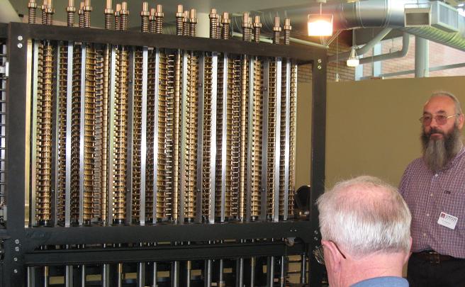
When I finished ogling wires, I took a look at Babbage’s Difference Engine No. 2. Designed by Charles Babbage in the 19th century, this massive mechanical marvel computes tables of polynomials. It supports up to 7th-order polynomials, and computes results to 30 decimal places. The desired polynomial is entered by setting a series of gears, and then a crank is turned by hand to generate the results, one at a time. Babbage designed it all on paper, and built working versions of small pieces of the mechanism, but it remained a purely theoretical invention for more than a century after his death. Some doubts remained about whether the machine would actually have worked, had it been built.
In 1985, the Science Museum in London set out to build a working Difference Engine No. 2, from Babbage’s original design drawings. The project took 17 years to complete, facing all sorts of setbacks, but in the end the machine worked as Babbage had intended. The finished difference engine is on display at London’s Science Museum, but a duplicate was made for project benefactor and Microsoft millionaire Nathan Myhrvold. Myhrvold agreed to lend his duplicate to the Computer History Museum, to share and educate.
Some of the other computing artifacts I got to see:
- Deep Blue, the IBM chess computer that defeated World Chess Champion Garry Kasparov in 1997.
- The first mouse- a block of wood with a momentary push switch mounted on it. Created by Doug Engelbart at PARC in 1964.
- A 10MB hard disk platter, 3 feet in diameter, from 1974.
- An original Apple I, the kit-built ancestor of the Apple II. A hand-assembled logic board, keyboard, and power supply, mounted on a plywood plank.
- A restored and working PDP-1. During the restoration, volunteers were able to retrieve data originally stored in the core memory decades earlier.
Too much awesome stuff!
Read 1 comment and join the conversation