Archive for May, 2010
Board Test Success!
Hot diggity damn, it works! It took me about four hours to fully assemble the Tiny CPU test board with all the components, which was good soldering practice. The surface-mounted navigation switch was a little challenging, but not too bad. Here’s how it looks after everything has been soldered in place:

I built the board up in stages, with stage one being the power section, and stage two being the JTAG header and CPLD socket. After that, I was able to connect the board to my PC, and get the JTAG programming software to talk to it successfully. With that first checkpoint passed, I was confident the rest of the assembly would go fairly smoothly.
Once the assembly was finished, verifying the correct function of the buttons, navigation switch, and LEDs only took a few minutes. The LCD and keyboard interfaces proved to be more challenging, since I had to implement the behavior using basic Verilog logic instead of any kind of microcontroller or CPU. I had hoped to make a demo of reading keys from the keyboard and echoing them to the LCD, but unfortunately that wasn’t possible, because there’s no on-board memory in which to store the scan code conversion table. Instead, I made a demo in which the keyboard scan codes themselves are displayed on the LCD.
Without any kind of on-board RAM or ROM, I felt like I exhausted the possibilities of this board pretty quickly. A 128 macrocell CPLD without other support logic just doesn’t do anything very interesting. I guess that’s fine, though, since the whole point of this exercise was to get some PCB design practice, and get the experience of building a real board before moving on to the more complex board needed for the full Tiny CPU design.
I predicted I’d find four mistakes in the board design, but I only found two issues that I would call “mistakes”. Fortunately I was able to work around them both. Aside from those mistakes, I also found several other areas in which the design could be improved.
Mistakes
Reset circuit – The reset IC I’m using has separate output pins for the reset and /reset signals. Reset is a standard logic output, but /reset is open drain, and requires a pull-up resistor. I missed that little detail, and didn’t include a pull-up. To work-around the problem, I bent the /reset pin up and cut it off, then jumpered reset to /reset on the underside of the board, and changed the CPLD logic to expect an active-high reset signal instead of active low. You can see the cut-off pin at the bottom-right of the photo above. It’s pin 6 of the DIP-8.
PS/2 connector footprint – The PS/2 connector I bought had three through-hole “feet” for mechanical stabilization, in addition to the six signal pins. The footprint I used in Eagle only has one foot. My fix was to cut the other two feet off before mounting the connector on the board, which sacrifices some stability, but has no other negative effects.
Areas to Improve
Edge placement – The JTAG connector, PS/2 connector, and power connector all hang slightly off the edge of the board, which wasn’t intentional.
Component spacing – Components are packed in a little too tightly in a couple of places. All those little 0.1 uF capacitors surrounding the CPLD socket have to bend outward slightly, because they rub the socket’s outer wall. In retrospect, I should have left a little more breathing room between everything when doing the layout.
Expansion header power – The expansion header on the left side of the board doesn’t have any power or ground connections, limiting its usefulness. Instead, all the expansion pins are connected to CPLD I/O pins. Oops.
Test points – I didn’t include any test points or convenient places to connect an oscilloscope probe or signal tester. At least a spare pair of power and ground pins would have been handy.
JTAG connector – It would have been better if the JTAG connector were rotated 180 degrees. In the current orientation, the cable has to drape over the board, instead of off its edge. You can see this in the video.
Signal trace to nowhere – I must have forgotten to clean up an old trace completely while I was routing. During assembly, I noticed this signal trace that leads nowhere.


Got Board
My “Tiny Board Test” custom-designed PCB is here! The BatchPCB order took 18 days from design submission to delivery, but it seemed like an eternity. It’s pretty awesome to see my ideas rendered in copper and fiberglass. Somebody might even mistake me for one of those professional electro-whatsit engineers. Shhh, don’t tell anyone I’m making it all up as I go!

I actually received two boards, although I only ordered one. This seems to be common with BatchPCB. Because they don’t perform any electrical testing on the boards, maybe they make up it for it by sending extras?
The drill registration on this board is not great. You can see in the photo that all the drill holes are offset slightly above-left of the pads, especially noticeable in the top-left corner of the board. It’s close enough that I think it should still work OK, though. The second board (not pictured) has much better drill centering. Both boards are routed with nice straight edges– it’s the extreme close-up perspective of the camera that makes the edges look curved here.
I did some cursory electrical testing, and everything seems fine. I guess there’s nothing for it but to solder on all the parts, and see if it works? Let’s take bets on how many errors I’ll discover in my original design during the assembly process. My guess is four!
Read 5 comments and join the conversationBits of Progress
Lots of good news on the Tiny CPU front!
I successfully programmed a Flash ROM via the JTAG indirect method today. Woohoo! I was never able to get it to work previously, and couldn’t figure out why. Several possibilities:
Comically long, loopy wires connecting the CPLD to the Flash? These were pretty much guaranteed to act as antennas and pick up noise. I replaced them with neatly wire-wrapped connections.
Questionable software? Previously I was using a demo copy of the commercial program TopJTAG Flash Programmer. When I tried to program the Flash, it would just time out. I switched to using a free, command-line JTAG/Flash tool called UrJTAG.
Unsupported Flash type? I switched to a 512KB AM29F040B, instead of the smaller capacity AM29F010B. I’m not sure it really mattered, but the AM29F040B was specifically mentioned as a supported Flash type for UrJTAG.
Unconnected VCCIO? The CPLD demo board I bought from eBay appears to have a design flaw. The VCCIO pins are all connected to each other, but not to anything else! I only discovered that by accident. I’ve now connected them to 5V.
I changed all four things at once, and now it works. The programming speed is about 400 bytes/second. That sounds pretty horrible, but it’s actually not bad. Programming an 8K block took 22 seconds to write, and an additional 16 seconds to verify. That’s plenty fast enough, so I don’t think I need a separate bootloader.
What’s even more exciting is that I got the ship confirmation email from BatchPCB today! That’s 15 days from design submission to shipped boards, which isn’t as bad as I’d expected it to be, but it still seemed like an eternity. This is only my test PCB, though: it only has a single CPLD (Tiny CPU will have two), and no RAM or ROM. It should prove that my basic PCB design will work, though.
Progress on “making things smaller” is going well too. I got some 32-pin PLCC Flash ROMs, which can still be unsocketed and put into a stand-alone programmer if necessary, but are only about a quarter the size of a comparable DIP. Here’s a comparison:

I’m also getting more confident in my surface-mount soldering skills, to the point where I’ll probably look at replacing some of the other components like the RAM with smaller, surface mount versions. Now that I’ve got JTAG indirect programming working, I could theoretically switch to an even smaller surface mount Flash ROM package too. I’ll probably keep the PLCC version, though, so I can retain the option for stand-alone programming in an emergency.
Be the first to comment!Maker Faire 2010
Ah, Maker Faire. It’s part garage inventions, part Burning Man reruns, part techno-supermarket, and all awesome. Can it possibly be a year already since Maker Faire 2009, where BMOW was featured in Wired, Slashdot, Digg, etc. and I talked myself hoarse in a 48-hour marathon of CPU conversations?
This year I headed back to the Faire as a visitor rather than an exhibitor, so I’d actually have a chance to see the cool stuff I missed last time. The show has actually grown since last year, which I didn’t think was possible, but they annexed a neighboring county or something and added even more exhibits than before. This event is big, big, big. It’s almost too big. After a few hours my brain was fried, and I just couldn’t appreciate all the awesome stuff anymore. I think there were at least three different robot death-matches, ten 3D printers, and dozens of Arduino add-ons.
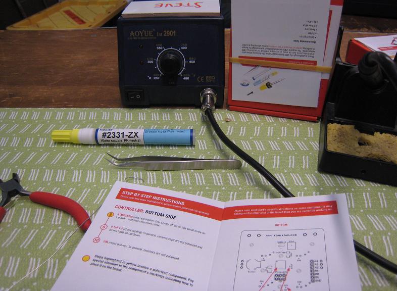
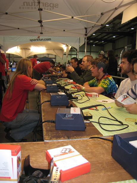
My major goal for the show was to do SparkFun’s SMD soldering class. I made a beeline to the SparkFun tent as soon as I arrived, and after a short wait, I sat down with eight other solder artists to construct SparkFun’s Simon kit. Here are a few pics of the setup:


After a short introduction, we jumped right in, and I soldered the first tiny IC without any problems (1 mm pin spacing). But at step two, a surface-mount capacitor, the wheels came off the cart. I just couldn’t get the cap to stick to the pad, after at least ten attempts, and eventually I overheated the cap to the point where it disintegrated. I sheepishly asked for a replacement, which took a while for them to find, and it took even longer for me to successfully solder it in place. Everyone else in the class was well ahead of me, and I was beginning to feel like a dummy.
After a few more steps, I soldered in the battery terminals, and was ready for the first major checkpoint: test for 5V. Unfortunately, this was when I discovered I’d soldered the battery terminals onto the wrong side of the board! One of the instructors took it to a rework station to fix it, which took a mysteriously long time, and when he came back I had a burned board with one trace lifted off the PCB. Argh. Eventually I was able to repair it with a jumper wire, and it passed the 5V test. But we were now an hour and a half into the class, and many of the other people were already done, just awaiting their turn to have the Atmega on their Simon board programmed.
I kept working, while the people on either side of me debugged their boards. After programming, one neighbor had a board where only two lights worked, and another had regressed and no longer passed the 5V test. While they debugged, I moved steadily forward, and eventually finished the assembly. At this point, both SparkFun’s main and backup Atmega programmers broke, and they were unable to program any more boards. Not a great ending to the class.
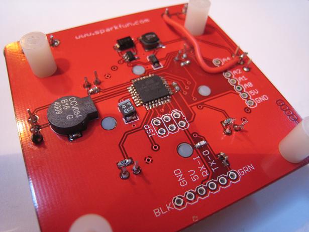
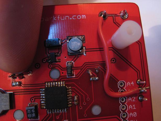
Ironically, the Atemga itself with its 0.65 mm pin spacing (I think) was actually pretty easy to solder. Just tack one corner, blob solder onto all the other pins while ignoring shorts, and then suck away the excess with solder wick. I’d say it’s the small size of the components that makes soldering them challenging, less so than the spacing of the pins. Take a look at these photos of my finished board. Some of those little surface mount passive elements are soldered in at awkward angles, but it’s the best I could do. Look at the size of my finger for reference. That tiny capacitor to the lower-right of the Atmega in the second photo is only about 1 mm long, and 0.5 mm wide… yikes! These parts make a grain of rice look giant. It’s tough to even see these things clearly. In the photo you get a pretty clear view, but with the naked eye that tiny cap is just an unidentifiable grayish speck, and whether it’s soldered properly is impossible to tell.


After the class, I wandered the Faire for most of the day, seeing lots of pretty cool stuff, but nothing that really stood out in my mind as exceptional. I enjoyed getting a chance to program an Altair 8800 using the front panel switches, but overall I think the show was just too much steam punk exploding fireball mechanical giraffe sensory overload.
As I prepared to leave at the end of the day, I stopped by the SparkFun booth once more, and they’d managed to get their Atmega programmer working again. I asked if they could program my board before I left, so I could attempt to debug the inevitable problems later at home. They did, but instead of a debugging puzzle, I got the happy “beep!” of a working Simon board. No debugging needed!
HUGE thanks to the SparkFun guys. The soldering class was great, and my instructors Matt and Matt were full of help and encouragement. The class itself was a fantastic bargain, since they only ask for a $20 donation, which goes to local science-related education projects. The Simon kit sells in the SparkFun store for $25, so this was like getting a $5 discount off the kit *and* free hands-on training. Can’t beat that!
Be the first to comment!Small ROM
In my ongoing effort to make the Tiny CPU board as small as possible, I’m looking for a small Flash ROM or EEPROM. That’s small in physical size, not necessarily capacity. My search has led me to examine many different ROM package types and interfaces, but unfortunately I’ve yet to find anything better than a standard Flash ROM in a 32-pin DIP package, using a space-hogging ZIF socket, with reprogramming performed by removing the ROM to a stand-alone programmer.
JTAG?
My dream solution is a programmable ROM with a JTAG interface. Then I could add the ROM to the JTAG chain, and program it using the same hardware and software I’ll already be using to program the CPLDs. Unfortunately, the only JTAG ROMs I’ve found are intended for use as FPGA configuration devices, and have a serial interface instead of the standard parallel address and data lines I need. They’re also surprisingly expensive.
SPI, I2C?
I’ve seen a couple of ROMs that use SPI or I2C for programming, but that doesn’t help me much. I don’t have any appropriate programming hardware, and at any rate these also don’t have parallel address/data interfaces. I do have an FTDI USB-to-serial cable, which might be usable for programming if I had appropriate software and a serial-programmable, parallel addressable ROM.
JTAG Indirect?
An approach with some promise is JTAG indirect programming, in which the ROM’s pins are connected to some other JTAG-enabled device, and then JTAG boundary-scan bit shifting is used to manipulate those pins to program the ROM indirectly. This might work, but available information and software for actually doing it seems scarce. I’d need some better examples, and some software that actually does indirect programming, before I could evaluate it. ROM programming using the JTAG indirect method is also reportedly slow, but just how slow isn’t clear. If it takes several minutes to program a 128K ROM, I would probably get annoyed.
Custom Interface?
I might use a standard Flash ROM in a smaller package, soldered directly to the board, and connected to a simple microcontroller or other device used to program it. That would be essentially equivalent to JTAG indirect programming, but rolling my own solution. The addition of a MCU or other programming hardware would mostly cancel out the space savings of the smaller IC package, though. Creation of a ROM-image loader also likely wouldn’t be trivial.
DIP.
It seems that all paths lead back to where I started: A plain old DIP, in a ZIF socket for easy plugging and unplugging. It will take up a lot of space, but I can easily transfer the ROM back and forth between the Tiny CPU board and my EPROM programmer whenever I need to update the ROM image. Maybe this is one case where the old, tried and true solution is best.
Read 16 comments and join the conversationCheetos Guitar Amp
Random project for a Saturday afternoon: a guitar amp in a Cheetos Crunchy can. I followed a modified version of Make Magazine’s cracker box amp design, which uses an LM386 power amplifier and a few passive components. The amp has separate crunch (gain) and volume controls, is powered from a 9V battery, and delivers half a watt through a 2-inch speaker hidden inside the can. The whole thing went together in a couple of hours, and most of that was planning how to arrange the parts.
Now I just need to learn how to play guitar.


