Separated at Birth
I’ve been planning to use an Altera Max 7128S for this CPLD – CPU project, because at 128 macrocells it’s the largest commonly-available CPLD that I could find in a PLCC package. Yesterday, however, I started wondering how the competition from Xilinx stacked up. Even if I couldn’t get as large a device (108 macrocells max in a PLCC package), maybe the Xilinx device architecture allowed for denser logic, more product terms per macrocell, or some other factor that might permit it to do more with less. So I read through the details of the Xilinx XC95108 CPLD datasheet, comparing it to the Altera EPM7128S CPLD, to see how they differed.
What I found nearly made me laugh out loud. They are the same. Not just similar, but virtually identical in their internal architectural details. All the marketing terms and sales claims make it sound as if each vendor has some amazing technological advantage, but it’s all just hype. Inside, when you look at how these devices work internally, there’s no meaningful difference I could find. What’s more, the descriptive text of the two datasheets is so similar, if this were a school project, they’d be hauled in front of the disciplinary committee on plagiarism charges.
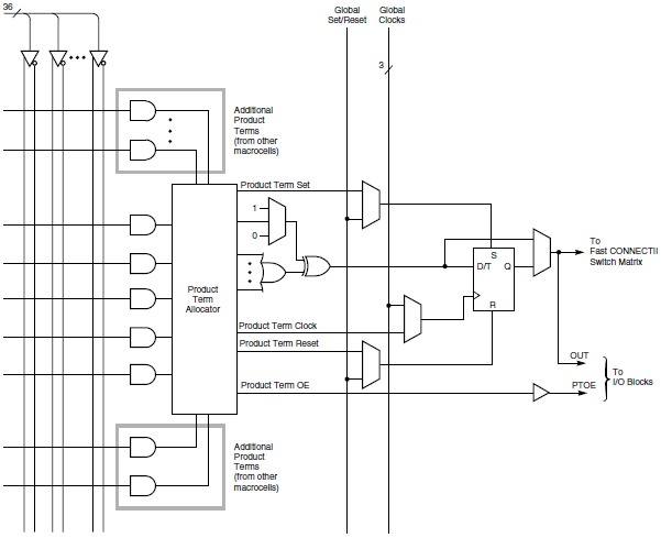
Take a look at the Altera diagram of one of their macrocells. You’ve got a logic array on their left with 36 inputs, five product terms feeding into a selection matrix. Additional product terms from other macrocells can also feed into the matrix if needed. The output goes to set of OR/XOR gates, and then either to a flip-flop, or bypasses the flip-flop and exits the macrocell. Product terms can also be used as clock, preset, clear, and enable control signals for the flip-flop, or global signals can be used for those controls.

Now take a look at the diagram of a Xilinx macrocell. Look familiar? 36-Entry logic array, five product terms, optional expansion terms from other macrocells, OR/XOR gates, flip-flop with bypass, and choice of product terms or global signals for clock, preset, clear, and enable. It’s almost an exact copy of the first diagram. It’s like a children’s game of “find five differences between these pictures”.

OK, there are some minor differences, like Altera’s “expander” product terms, and the exchange of a clock enable for an output enable signal. But you have to admit these diagrams are so similar, they could have been made by the same person. They even make the same arbitrary choices for orientation and position of the elements in the diagram.
Now compare the accompanying text. First, Altera’s: “Combinatorial logic is implemented in the logic array, which provides five product terms per macrocell. The product-term select matrix allocates these product terms for use as either primary logic inputs (to the OR and XOR gates) to implement combinatorial functions, or as secondary inputs to the macrocell’s register clear, preset, clock, and clock enable control functions.”
And here’s Xilinx’s text: “Five direct product terms from the AND-array are available for use as primary data inputs (to the OR and XOR gates) to implement combinatorial functions, or as control inputs including clock, set/reset, and output enable. The product term allocator associated with each macrocell selects how the five direct terms are used.”
Don’t those seem more than just a little bit similar? I mean, there’s a long clause that’s almost word-for-word identical, including the choice to use a parenthetical expression: “for use as [either] primary [logic/data] inputs (to the OR and XOR gates) to implement combinatorial functions, or as [secondary/control] inputs”. That can’t be a coincidence.
Read 2 comments and join the conversation2 Comments so far
Leave a reply. For customer support issues, please use the Customer Support link instead of writing comments.


Interesting. I’d never thought to compare their product lines so closely. I knew they were similar, but I never realized how similar.
I wonder if Xilinx and Altera are essentially sellings licensed CPLD cores? CPLDs are not their high margin parts and probably not where there is much in the way of innovation for them. If they consider CPLDs a “solved problem”, then why not license them (either to others or from others)?
Then again, it is possible that they are both optimizing for the same problem and end up at basically the same place. But… Yeah… The number of coincidental choices that would require to end up so similar *seems* improbably high.
Also meeting your requirements (128 macrocells, PLCC packaging) is Atmel’s ATF1508. It has basically the same macrocell structure as the Altera and Xilinx parts you’ve shown (5 product terms with optional cascading, followed by OR, XOR, FF and lots of muxes). It does have an additional feature that caught my attention: it can dedicate one of the product terms to the FF input and let the output of the XOR gate route to the output of the macrocell. Both the macrocell output as well as the FF output independently feed back to the routing matrix. Thus you can use the macrocell for both a simple register as well as unrelated combinatorial logic simultaneously.
The overall similarity between these parts certainly make it clearer to me why Atmel labels the family that the ATF1508 comes from as “industry standard compatible”. I had wondered what this meant since they never seemed to actually specify a standard by name. They probably just want to be able to tempt each other’s customers away with promises of “painless” product substitutions.