Archive for April, 2008
USB Action
BMOW is now USB-enabled for PC communication, for both reads and writes. Yahoo!
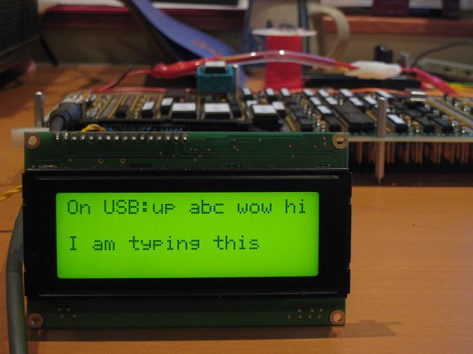
I wrote a simple program to log when the USB interface goes up and down, and to echo all bytes received from the PC to BMOW’s LCD. The program also adds one to each received byte before transmitting it back, so I could prove it was transmitting real data and I wasn’t seeing some local echo. The result was that whatever letter I typed on the PC, the next letter of the alphabet got sent back in reply. Here’s the Windows Hyperterminal session:

The whole exercise went very smoothly, and I didn’t have to do any debugging at all. Once I got the USBMOD4 in place, it all worked on the first attempt you see here.
The only wrinkle was with the USBMOD4 itself. I bought one months ago that was damaged in shipping: some pins were broken off. Futurlec sent me a replacement, but I didn’t open it until yesterday, only to discover it was the wrong part! After scouring the USBMOD4 data sheet, I worked out a modified solution that let me use the damaged module, which was only possible because all but one of the broken pins were ground pins. I ended up needing to desolder a SMD component on the USBMOD4 body, which was ugly, and I was also forced to use the integrated USB jack rather than the external USB jack I’d planned on. But I can live with the little flaws… and hey, now I’ve got USB!
Read 1 comment and join the conversationValidation Test
Remember that validation test suite I wrote last December? Back then, I ran it using a Verilog hardware simulation of BMOW, and it exercised every variant of every machine instruction: adds, jumps, xors, loads, stores, branches taken, branches not taken, branches forward, branches backward, branches across a page boundary, and on and on in mind-numbing variation. Now I have that same test running and passing on the real BMOW hardware! OK, I had to cheat a little and disable the stack-related tests, since I still haven’t wired up the stack pointer register. But the other 95% of the tests run perfectly and the LCD says “pass”. Things are really looking good!
The stack pointer is the next obvious step. I’m a little hesitant to do the wiring, since the last two pieces of hardware that I added each made the machine stop working, and led to frustrating debug sessions. Hopefully this time will go better. Then the core “computing” part of the computer’s hardware will be done, and I can begin on I/O (keyboard, USB) and the real-time clock.
Read 3 comments and join the conversationRAM Test
Egads! The RAM works. This thing is starting to look like a real computer now. I wrote an improved version of my fibonacci program that operates on 16-bit values, using 4 bytes of RAM as temporary storage. I then created a super-program by combining the 16-bit RAM-based fibonacci with my earlier 8-bit fibonacci that uses only the A, X, and Y registers, as well as the “BMOW is alive!” program. At bootup, the super-program checks the value in the A register and uses it to choose one of the three demo programs to run. Each demo program writes a new value into A before halting. Since A isn’t cleared when the machine is reset, every time I hit the reset switch it runs the next program in the demo loop. Woohoo, user interactivity! Here’s a photo after running all three:
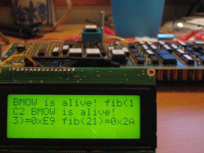
I’m using the 20×4 LCD now instead of the 16×2 one from the earlier photos. The fibonacci results are written in hexadecimal, since it was easiest for me to generate. The text is a little hard to interpret, because the LCD is mapped as two logical lines, where the first logical line covers the first and third physical lines of the LCD, and the second logical line covers the second and fourth physical lines. It reads “BMOW is alive! fib(13)=0xE9 fib(21)=0x2AC2 BMOW is alive!”
Some system facts:
- Current clock speed is 1MHz. It should be able to go faster ultimately.
- 512 KBytes of RAM, 16 KBytes of ROM.
- Power draw is 8 Watts, implying 1.6A at 5V.
- There are presently 704 connecting wires, so 1408 individual wire wraps.
It’s been a while since I posted any photos of the overall construction progress, so an update is overdue.

Here’s a close-up of the wire-wrap side of the board. Things are getting a little crazy. The photo doesn’t do justice to the fine detail of the dense wiring. Wires are stacked 10 deep in some channels! Big Mess o’ Wires indeed.
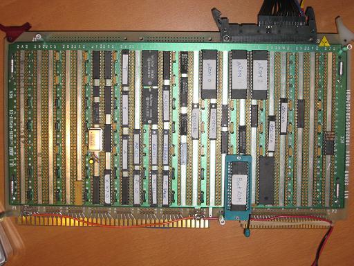
The component side is well-populated now. Eventually the rest of the bottom and right side of the board will be filled. The left side will be available for any possible future expansion, like audio or video.
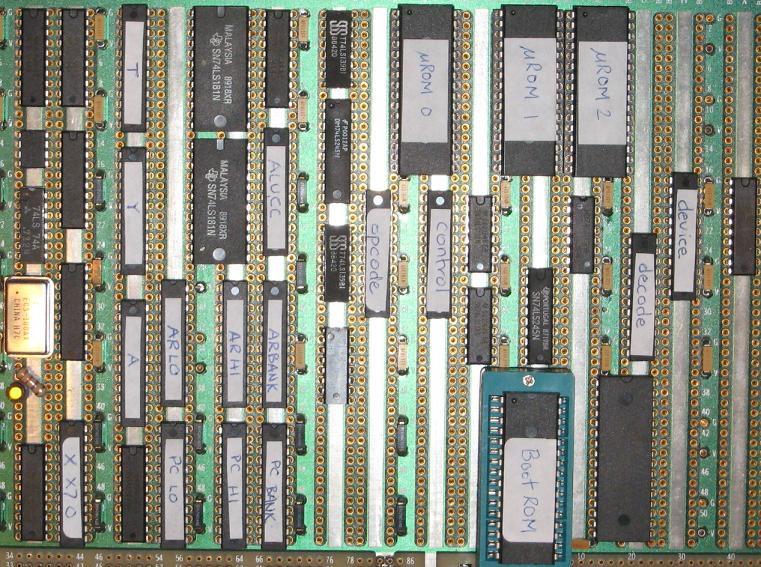
Here you can see the three micro-ROMs at the top, and boot/program ROM below. That’s the newly-installed RAM immediately to the right of the boot ROM. All of the narrow chips with white labels are GALs. The rest of the unmarked chips are various 74LS series logic parts. Since there’s no fan or other moving parts to make an obvious noise, I added the yellow LED below the clock oscillator to remind me when BMOW is on.
Read 2 comments and join the conversationMore Hardware Woes
After my earlier hardware glitches were seemingly resolved, I added the RAM to BMOW, which is the last of the basic hardware components needed. Unfortunately, this created a huge new set of hardware problems that I can only describe as “everything’s broken.” I haven’t even attempted to use the RAM yet, but its mere presence in the system (and the wires connected to it) seems to have caused everything to go haywire, and now the old “BMOW is alive!” program no longer works at all. I haven’t had time to really nail down what’s going wrong yet, but there are so many signals that suddenly seem to intermittently get the wrong values, I feel like my whole house of cards has just collapsed.
Update: A ROM was loose. D’oh! BMOW is alive, again.
Hardware Glitches
Just after I wrote last week’s entry, the hardware went from proudly proclaiming “BMOW is alive!” to merely stating “BMOW is aliv”. I was able to track this down to a problem with the program counter chip. Often, but not always, the low byte of the PC would roll over from FF to 01 instead of 00, and continue counting from there. The lowest bit of the address, A0, seemed to get stuck at 1 during a rollover. That wasn’t too painful to diagnose, but understanding *why* it was skipping 00 and how to fix it proved to be a much bigger problem.
The PC is implemented as a GAL, so the first thing I did was try replacing it with a new GAL, on the theory that the chip was bad. No help. Then I double-checked my GAL equations, and the raw fuse map produced by the GAL assembler, looking for errors. I found none. It seemed that the problem wasn’t simply bad hardware, nor a flaw in the logic, but some kind of electrical/noise/timing problem. Exactly the sort of problem I fear the most.
I checked every pin on the chip with my oscilloscope, looking for obvious spikes, noise, or power sags, but everything looked pretty good. There was some noise on some of the data load inputs, but nothing egregious, and those inputs aren’t used when incrementing the PC anyway. The scope showed that during a rollover, when A0 should have transitioned from a high voltage to a low one (1 to 0), it would start to dip low for about 5ns, then suddenly pop back up to a high voltage.
I tried slowing the system clock all the way from 1MHz down to 250kHz without success. I modified the GAL programming to make the PC increment every clock cycle, ignoring the count enable input. Of course this made the machine totally non-functional, but the rollover bug still occurred, as demonstrated with the scope. I tried removing all the other chips connected to A0, but the problem still persisted, and now the machine was even more non-functional.
Finally I tried rewriting the GAL equations to move A0 to another output pin, and the problem followed A0 to its new pin. This seemed a key bit of evidence, suggesting that the problem was not with the pin itself, nor the wires connected to the pin, but with the logical quantity A0. That led me to ask what was different about A0 versus A1-A7, which didn’t exhibit any problems. The answer is that when counting is enabled, A0 always changes state: a 0 becomes 1, or a 1 becomes 0. The other bits only change state depending on the values of the lower bits. In short, the PC was acting exactly as if it were being clocked twice in rapid succession.
I jumped back to the oscilloscope, looking carefully at the clock input to the PC at the moment of rollover. The clock looked fine, in fact it looked very clean. My scope only has 5ns timing resolution, though, so if there were a glitch of less than 5ns on the clock line, it might not show up. I wondered if there was a way to avoid a double-count in the case of a double-clock. I came up with the dangerous-sounding idea of including the clock itself in the product term used to compute the new A0 value at a clock edge. This certainly feels strange: by definition the A0 value will change exactly when the clock transitions from low to high, at which point the clock-as-data value will be undefined. The GAL program change also involved switching the A0 equation from negative logic to positive. Here it is (note the /clk0 term in the new equation):
| ; old equation |
| /q0 := /_reset + _reset*_cnt_in*_ld*/q0 + _reset*/_ld*/d0 + _reset*_ld*/_cnt_in*q0 |
| ; new equation |
| q0 := _reset*_cnt_in*_ld*q0 + _reset*/_ld*d0 + _reset*_ld*/_cnt_in*/q0*/clk0 |
This worked. So the problem has been successfully papered over, but not really solved. There are a couple of other experiments I’d like to try, in order to better understand what’s happening:
- Try a quarter-power GAL instead of my low-power ones. Perhaps the surge in power when all the address lines simultaneously switch from 1 to 0 is causing the clock glitch I can’t see. If so, a more power-efficient GAL might help. I’ve got one on order.
- Try a 15ns GAL instead of my 25ns ones. I don’t think the propagation delay has anything to do with the problem directly, but perhaps the different internal structure of the 15ns GAL would exhibit different symptoms. I’ve ordered one of these too.
- Experiment with various methods of terminating the clock line.
Termination seems to be something of an inexact process, from what I’ve read. I tried connecting a pin somewhere midway along the clock line to ground, through a 220 Ohm resistor, and it made the clocking problems worse. I’ve seen other designs that use an in-series resistor of around 40-80 Ohms, rather than a resistor tied to ground. I’ve been unable to find much good discussion of the need and method of termination for TTL circuits running in the 1-4 MHz range, and most of what I have read talks about terminating signals on the bus or backplane, which I don’t have. If anyone reading this knows more about this and could offer some advice, I’d love to hear it.
Update: Some more details on the PC clock may be useful for termination analysis. The low byte of the PC is computed by the GAL called PCLO in the schematics. It’s using the clock line Q0B, which is output from a 74LS244. Q0B is transmitted along a chain of wires about 21 inches in total length. The ‘244 that outputs the clock is at the beginning of the chain, and PCLO is about 9.5 inches down the chain from the ‘244, and about 11.5 inches from the end of the chain.
The clock signal propagates past PCLO, 11.5 inches to the end of the chain, reflects off the end, and propagates 11.5 inches back. So the reflected signal must travel 23 inches, or about 0.6 meters. Assuming 5 ns per meter signal propagation in copper wire, the reflected clock signal will arrive back at PCLO in 5 * 0.6 = 3 ns after the original signal. Maybe that causes the double-clocking?
Read 4 comments and join the conversationBMOW Is Alive!
Everything seems to be falling into place now. I think a picture says it best:
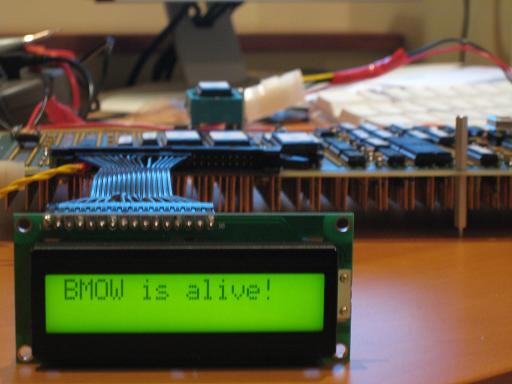
The LCD is up and running, displaying messages from the ROM program. I wasn’t lucky enough to have it work on the first try this time, though. I had to debug some accidentally swapped address lines and some uninitialized registers, but after a few hours of fiddling, I was rewarded with the greeting in the photo.
I’m starting to realize a few bad points about my physical setup. The biggest headache is getting chips in and out of the wire wrap board to reprogram them. They’re always hard to remove, and even with a chip puller, I’m afraid I’m going to damage or break a pin when the chip suddenly dislodges. I have my boot ROM in a ZIF socket, but all the microroms are in standard (non-ZIF) sockets, and the GALs aren’t socketed at all. What’s worse, the microrom sockets don’t seem to be making a consistent contact with the board. In one case, I was able to toggle the machine between working and not working just by pushing down on one of the microrom sockets a little. This is the sort of random, elusive electrical problem that worries me far more than any design problems.
Things are getting to the point where I really need a case or cabinet of some sort. I don’t necessarily want to put it in the PC case yet, since then I’ll have to be constantly removing it to work on the hardware. But the naked wirewrap board with power, reset, and LCD cables hanging off in random directions is getting pretty unwieldy. I’m thinking about constructing a temporary “development” case that’s more like a frame. It would provide something to easily grip everything by, and a place to anchor the cables and connectors, but still be totally open at the top and bottom. I’m hopeless with machine tools, but maybe I can cobble something half-respectable together with some scrap wood and screws.
Read 2 comments and join the conversation
