Archive for March, 2008
Funny Fanout Flaws
Ugh, I’ve run into my first design flaw. Fortunately, I don’t think it will be too difficult to fix, but it’s an eye opener nonetheless.
The issue I’m facing is fanout limitations. Fanout is the number of inputs that are connected to an output. Say I’ve got a chip that outputs some data signal, and that signal is passed as an input to ten other chips, then I’ve got a fanout of 10.
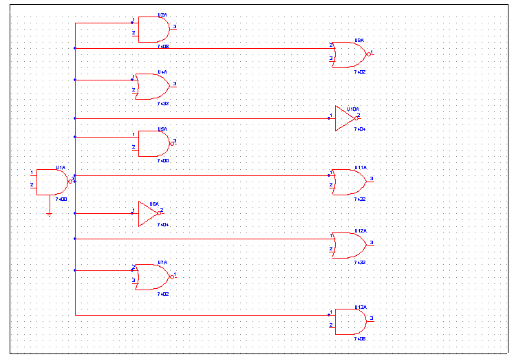
So what’s this about fanout limitations? Can’t you connect as many inputs as you’d like to that data ouput? To understand fanout limitations, it’s necessary to leave the cozy digital world of zeros and ones, and consider the analog nature of the circuit. In the case of a logical “1” at the data output, the output chip attempts to bring the output pin to 5 volts, or something close to it. A small amount of current then flows from the output pin to the input pins. In the case of TTL logic (the 7400 family), as long as the voltage at each input pin is over about 2.4 volts, the input chip will treat it as a logical 1. This allows for a certain amount of loss or noise in the circuit between the output and inputs.
Unfortunately, there is always a small amount of internal resistance in the output chip, between the power supply and the output pin, of something on the order of 10K ohms. Let’s say that an input pin draws 20 uA of current, so from Ohm’s law, V = IR, we can calculate an expected voltage drop of 10KOhm * 20uA = 0.2 volts. So with one input connected, the voltage at the output pin won’t actually be 5 volts, it will be 5 – 0.2 = 4.8 volts. As more inputs are connected, the current will increase, and so will the magnitude of the drop below 5 volts. At some point, if enough inputs are connected, the output voltage will sag below the 2.4v threshold needed for a valid logical “1”, and the circuit will stop functioning correctly.
In reality the situation is somewhat more complicated than I’ve described, as the input resistance needs to be considered too, and in fact TTL outputs never drive all the way to 5 volts anyway due to their design. However, the basic conclusion remains the same: connect too many inputs to a single output, and things will go bad. For TTL logic, the generally accepted limit is 10, although it varies from chip to chip.
Examining my schematics, I realized that they call for 10 different chips connected to my memory data bus, and I plan to add one or two more before the project’s completion. That translates to a fanout of 9 to 11 for each of the bus’ data lines. Maybe that would work fine, maybe not, but I don’t really want to find out. With my luck it would kind of work, some of the time, and I’d never be able to figure out what was going on.
My plan for reducing fanout on the memory data bus is to connect all the “write-only” chips (opcode, LCD, and eventually sound and video) to a 74LS244 bus driver, and then connect that driver to the main memory data bus. That will bring the fanout down to 8, even in the worst case if I do add those extra chips. Isolating the read-only and read-write chips should be possible too if it proves necessary, but it would involve using some glue logic to combine various output enable signals, and bidirectional bus-drivers, and other headaches I’d just as soon avoid if I can.
Be the first to comment!Bit by Bit
Although progress continues to be slow, the machine is taking shape bit by bit. I bought another 100 foot spool of wire, along with 1000 pre-cut and pre-stripped wires in lengths from 1 to 4 inches. The pre-cut wire makes the job go considerably faster, not only because it saves me from cutting and stripping, but also because consistent length wires are easier to wrap and bend into place on the board.
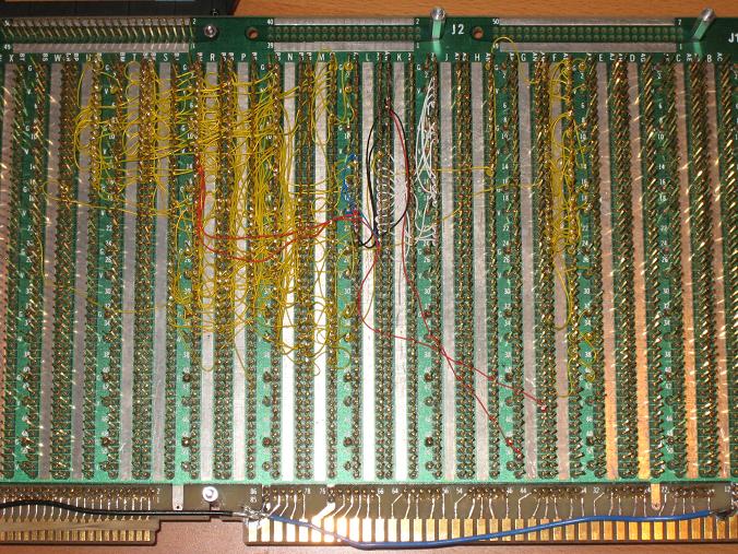
Big Mess o’ Wires is finally starting to live up to its name! Just look at that mess. My first spool of wire was yellow, and all of the clock and control system connections used the yellow wire. The pre-cut wire I’m using now is a different color for each length: white is 2 inches, black is 2.5 inches, and so on. That gives the board a multi-colored appearance that looks like a mess, but is actually easier to navigate visually than a uniform field of yellow.
The /DRALU problems seem to be gone, now that I’ve made the connections between the ALU system and control system, meaning there are no more floating inputs on the control ROMs. I tested everything out with the logic analyzer again, and it seems OK, although there’s still not much to test with this half-built machine.
At this point, the clock/reset, control, and ALU systems are complete, and I’m getting close to the point where this pile of chips and wires may be able to do something interesting. My next steps will be to add the program ROM, address decoder, program counter, and a few related buffers, and see if I can execute a series of opcodes from the program ROM. Assuming that much works, I’ll add one or two of the registers, and primitive computing should then be possible.
Read 3 comments and join the conversationSlow and Slower
My recent wire-wrapping progress has been painfully slow: I’ve timed myself at about 2 minutes per wire. You might wonder how it could possibly take that long, but all the measuring, stripping, threading, wrapping, and squinting time really adds up. But despite my slow speed, I’m still moving steadily towards a working homebrew CPU.
Yesterday I finished the control section, which is the most complicated part of the CPU. That puts me somewhere in the 25% to 30% range for total CPU completion. As I was nearing the end of the control section, I realized I was running out of wire, and began to worry that I would run out before finishing the last connection. As it turned out, I finished the control section with a bare spool and about 2 inches of wire remaining. Now I’m on a forced hiatus until my replacement wire stock arrives.
The control section by itself doesn’t do much, since there’s no program for it to run, and no registers, ALU, or memory for it to control. But due to some lucky accidents, I was actually able to run and test a program of sorts. Here’s a photo of the setup:
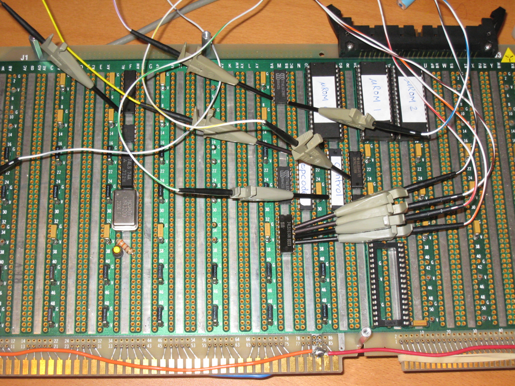
There’s no program ROM, so nothing from which to load opcodes. The opcode register with unconnected inputs appears to default to an opcode of 0xFF, so I programmed the micro-ROMs with a test micro-program for that opcode. My test micro-program exercises all of the various control output signals, which don’t currently do anything. However, I was able to verify their operation with the logic analyzer, and make sure everything is working so far.
I only ran into one problem, with the /DRALU signal that will drive the ALU output. Occasionally it’s a 1 when it should be a 0. More careful examination showed that the bogus 1 value only ever appears immediately after a valid 1, as if it were “stuck” on 1 for an extra clock cycle. The problem also only happens within the first second or two after power-up. After that /DRALU always looks fine, even if I reset the CPU while keeping the power applied.
I also looked at the /DRALU signal with the oscilloscope, and it goes from a nice clean 0 volts for a logical 0, to a nice clean 5 volts for a logical 1, to OH DEAR GOD horrible noise for one clock cycle, then back to a clean 0 volts. So clearly there’s noise that sometimes causes what should have been a 0 to become a 1, but I’m not certain why.
My first guess was a bad/flaky connection on one of the /DRALU pins. However, I can’t see why a flaky connection would only be a problem during the first couple of seconds after power-on, and only during certain clock cycles. And once the machine was warmed up, I wasn’t able to reproduce the problem, no matter how much I jiggled the board, chips, or wires.
My second guess was that I was getting unpredictable behavior, because some of the micro-ROM address inputs are still unconnected. However, the data in the micro-ROM is organized such that the data value will be the same regardless of whether those unconnected address inputs are 1’s or 0’s.
Once I get more wire, I plan to connect up the remaining unconnected micro-ROM address inputs, and see if the problem goes away. If not, I’ll try cutting out and re-wrapping the wires that carry the /DRALU signal. If that still doesn’t fix it, then I’m going to be in for some difficult debugging.
Read 5 comments and join the conversationConstruction
After ages of procrastination, I’m finally making some slow but measurable progress towards turning my paper design into reality, and actually building this crazy machine. Wire wrapping seems impossibly slow and tedious compared with working on a protoboard. Just creating a wiring list from the schematics is taking me lots of time, and the task of physically wrapping the wires isn’t speedy either. Nevertheless, I finished the entire clock generation system and verified that it works. I’d estimate that I’m about 5 or 10 percent done with the whole job, which doesn’t sound like much, but is still far better than zero!
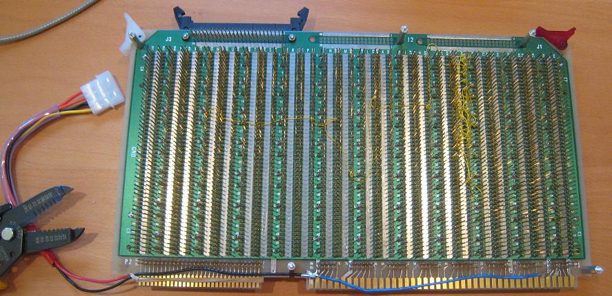
It was tough to get a clear photo of the wire side of the board, but here you can see what’s going on. The tangle of yellow wires near the right side is the clock generation system, and the yellow wires snaking off towards the left carry the clock signals for the chips. Eventually the entire board to the left of the clock generation system will be filled with wires, so that gives you an idea of how far I still have to go.
Hanging off the left, you can also see the 4-pin molex connector I attached for the power supply. It’s a standard PC power supply connector, like the type you’d use for a hard drive or case fan, so eventually I’ll be able to drop the board into the PC case I bought. I’ve also rigged up an adapter (not shown) that lets me connect the board to a simpler wall-wart power supply.
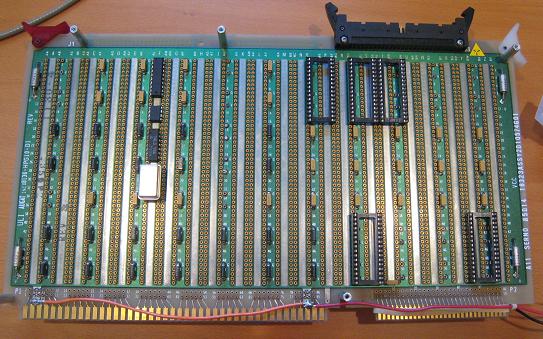
Here’s the component side of the board. You can see I’ve soldered in capacitors between power and ground nearly everywhere. The power filter caps are all those little vertical black or yellow boxes. You can also see the components of the clock generation system in column F, and the ROM sockets.

Here’s a shot of the clock signal at the end of that wire daisy-chain. Looks pretty clean. Of course there are no components connected to the clock yet that might screw up the signal, and this is also with a 500kHz clock rather than the intended 3MHz clock. Hopefully the clock signal won’t degenerate into unrecognizable noise by the time everything’s finished.
I wonder if it would be better to use CMOS components to generate the clock signal instead of TTL, since they’d drive all the way to 5 volts, and so would presumably help with any future noise problems. You can see here that the clock signal only goes to about 4 volts during the high portion.
Read 2 comments and join the conversation

