

Archive for the 'BMOW 1' Category
Construction
After ages of procrastination, I’m finally making some slow but measurable progress towards turning my paper design into reality, and actually building this crazy machine. Wire wrapping seems impossibly slow and tedious compared with working on a protoboard. Just creating a wiring list from the schematics is taking me lots of time, and the task of physically wrapping the wires isn’t speedy either. Nevertheless, I finished the entire clock generation system and verified that it works. I’d estimate that I’m about 5 or 10 percent done with the whole job, which doesn’t sound like much, but is still far better than zero!
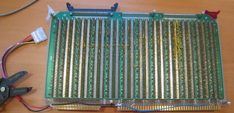
It was tough to get a clear photo of the wire side of the board, but here you can see what’s going on. The tangle of yellow wires near the right side is the clock generation system, and the yellow wires snaking off towards the left carry the clock signals for the chips. Eventually the entire board to the left of the clock generation system will be filled with wires, so that gives you an idea of how far I still have to go.
Hanging off the left, you can also see the 4-pin molex connector I attached for the power supply. It’s a standard PC power supply connector, like the type you’d use for a hard drive or case fan, so eventually I’ll be able to drop the board into the PC case I bought. I’ve also rigged up an adapter (not shown) that lets me connect the board to a simpler wall-wart power supply.
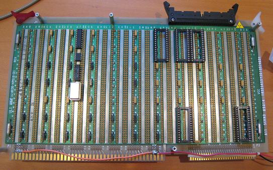
Here’s the component side of the board. You can see I’ve soldered in capacitors between power and ground nearly everywhere. The power filter caps are all those little vertical black or yellow boxes. You can also see the components of the clock generation system in column F, and the ROM sockets.

Here’s a shot of the clock signal at the end of that wire daisy-chain. Looks pretty clean. Of course there are no components connected to the clock yet that might screw up the signal, and this is also with a 500kHz clock rather than the intended 3MHz clock. Hopefully the clock signal won’t degenerate into unrecognizable noise by the time everything’s finished.
I wonder if it would be better to use CMOS components to generate the clock signal instead of TTL, since they’d drive all the way to 5 volts, and so would presumably help with any future noise problems. You can see here that the clock signal only goes to about 4 volts during the high portion.
Read 2 comments and join the conversationPeripherals Galore
There’s been lots of recent activity on different fronts. Too bad I still haven’t made any progress actually building the machine.
Keyboardin’ Part 2
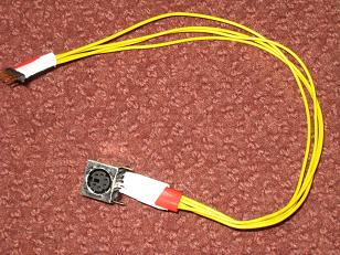
Here’s a shot of my glorious hand-wired PS/2 keyboard connector. I spent some time over the weekend working out the details of how to read keyboard data. I came up with a solution that uses a 74LS161 to count the incoming bits, and a GAL to shift the bits into a byte, and signal a CPU interrupt once all the bytes have been read. It should be pretty simple to use in practice. At first I was worried that my CPU wouldn’t be able to process interrupts from the keyboard quickly enough, and I’d need to implement some kind of queue for incoming keyboard bytes. After doing some testing, though, it turns out that there’s always at least 3 milliseconds between bytes, even for the bytes in a multi-byte scan code for a single keypress. That’s an eternity in computing terms.
Keeping It Real-Time
I ordered a Texas Instruments real-time clock from a parts supplier, and updated my design to incorporate it. Unlike most RTC’s I’ve seen that use the same pins for address and data (is this how “real” PC’s work?), this one has separate pins, and can be accessed just like a 16-byte RAM. It also has an integrated timer crystal and battery. Getting the current date and time is as easy as reading from a particular memory address. The RTC can also be configured to generate a periodic interrupt at intervals between 30 microseconds and 500 milliseconds, or at a specific future time.
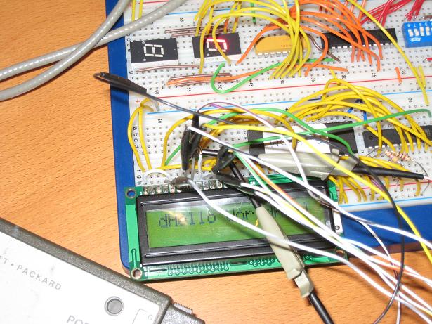
Embiggen My LCD
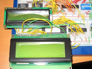
I got a new 20×4 LCD panel to replace my old 16×2 one. The photo above shows their relative sizes. Conveniently, the new LCD uses the same controller chip as the old one, so I was able to drop it into my existing “Hello World” circuit, and get it to print text on the LCD immediately. The LCD display panel’s height is almost exactly the same as a 5 1/4″ drive bay opening on a standard PC case.
On the Case
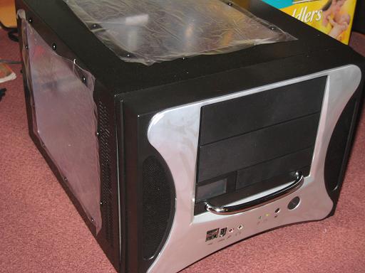
I decided to give up on the idea of building a custom case for BMOW. I’m having enough trouble getting motivated to build the machine itself, so I don’t need a case construction project too. I bought a standard PC case from Apevia, with clear side panels so that everyone can see my awesome hand-wired circuitry inside. The LCD should fit nicely in the lower of the two 5 1/4″ drive bays, and I can use the existing USB connector and power supply… sort of.
If you stop to consider how your PC is able to turn itself off from software, then you realize there must be something special going on with the power supply. It turns out that for a standard ATX power supply, there are some pins on the motherboard connector that a normal PC uses to tell the power supply when to turn on and off. The power button on the front of the case is connected to the motherboard, not the power supply. This means that if you don’t have a standard PC motherboard, you can’t actually turn on the power supply! This was a problem I hadn’t expected.
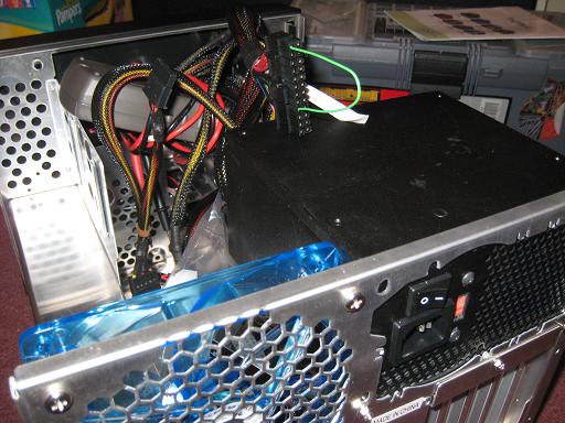
After some research, I learned that by inserting a jumper wire between two pins on the ATX motherboard connector, I could simulate the signal that a PC motherboard sends to turn on the power supply. It seems a little ugly and potentially dangerous, since connecting to the wrong pin could bridge different voltage outputs, or short power to ground, probably killing the PSU. Did you know that a standard PC power supply puts out 6 different voltages? +5v, -5v, +12v, -12v, +3.3v, and +5v standby circuit. On mine, several of these outputs can drive over 20 amps, which is enough to do some damage if I screw up the wiring. Nevertheless, I popped in the jumper wire, and it worked flawlessly. Above is a photo of my handiwork: a green jumper wire sticking out of the ATX connector above the PSU.
Beep Beep Beep
Like all PC cases, this one has a two wire speaker that’s normally used to make a “beep” at boot-up, and that’s all. I was curious how it worked. Did applying a voltage across the two speaker leads make it play a fixed frequency tone, or could I play any frequency tone by applying a varying voltage to the leads? It turned out that the speaker can play any frequency, with an appropriate input. This opens up a lot of interesting possibilities. By connecting just two more wires to my CPU, I can play arbitrary sounds!
The simplest approach would be to have the CPU set a speaker value in a dedicated audio register, which would be turned into an appropriate speaker voltage by a D-to-A converter. To play a sound, the CPU would need to quickly and continuously change the value in the speaker register, to create an output waveform. I don’t think BMOW will be fast enough to make this really practical, though. Assuming a modest 10kHz sampling rate for audio waveforms, and a 3MHz CPU speed, there would be only 300 clock cycles between each required update of the speaker register. That probably wouldn’t leave the CPU enough time to do anything interesting besides sitting in a busy loop, playing back a waveform.
A more realistic idea would be to have the CPU write the desired tone frequency to a speaker register, and then use dedicated hardware to generate a square or sine wave at that frequency. This would require very little CPU time, although the type of audio it could generate would be fairly primitive. Still, since this is a computing project and not an audio one, it seems like the best approach. I haven’t worked out the details yet, but I will probably divide the system clock down to about 10kHz, and then use the speaker register’s value to divide it down further by a variable amount, to produce different frequencies in the audible range. If I want to get fancy, I may also add volume or envelope control. I need to find a reasonable compromise between design complexity (not to mention part count) and the quality of sound I can generate.
Video Madness

After all this, I realized that I now had the makings of keyboard input, a nice case, and even audio output. All I was missing was video output to make a “real” computer, and ditch the USB link to a PC entirely. With that goal in mind, I started to research what it would take to generate NTSC or VGA video output from BMOW.
In short, while it would be complicated, I believe video output is within reach if I want to spend the time to do it. It’s silly, but video generation feels a little like the holy grail of computer design to me. Back in college, I actually built a primitive video game with NTSC output, and I still have all the circuit schematics. The video generator chip I used is now obsolete, sadly, and I couldn’t find any replacement. But as the number of devices I own that will display a composite video signal dwindles, it probably makes more sense to pursue VGA output rather than NTSC anyway. My investigations suggest that it’s about the same difficulty either way.
From what I can tell, there are five signals on the VGA connector that I would need to care about: horizontal sync, vertical sync, and red, green, and blue data. HSync and VSync are basically just square waves with non-uniform duty cycles, used to signal the start of a new line or a new frame. It shouldn’t be too hard to build a circuit using some counters to generate those signals, I hope, or I believe there are also single-chip solutions that generate the necessary sync signals. Then the three color signals are continuously varying analog voltages (between 0 and 0.7v, I think) during a portion of time between hsyncs. For a 640×480 output, the visible portion of each scan line takes about 25 us, or about 40 ns per pixel. A D-to-A converter could be used to generate the desired voltage output by reading a byte from a RAM every 40 ns, and converting it to color voltages.
After reading the VGA specs, I think it would be relatively straightforward to build a circuit to output a fixed VGA signal, in some kind of test pattern. While it certainly wouldn’t be a piece of cake, it would be just a matter of generating the appropriate sync and data signals. What seems much more complicated to me is sharing video memory between the video output circuit and the CPU. The video output circuit would always be reading successive bytes from the video RAM. So what happens when the CPU wants to write data to video memory? I can think of a few possible solutions, none of which seem great:
- The CPU takes priority over the video output circuit, pre-empting it. Some kind of video garbage gets rendered very briefly if this happens during the visible portion of the VGA screen refresh.
- The CPU waits until a horizontal or vertical blanking interval, and then writes its data. This would avoid video garbage being drawn, but stalls the CPU, and requires implementing some way for the CPU to query the video circuitry state.
- The CPU writes data to a video input FIFO instead of directly to video memory, and the video circuitry drains the FIFO during the idle of blanking intervals. This would work well, I think, but would be complex to implement. The CPU would still have to check to make sure the FIFO wasn’t full before writing new data.
- The video circuitry stores data in a video output FIFO, rather than transferring data from video memory directory to the D-to-A converter. This would be very similar to the previous approach, although perhaps slightly easier to implement, since it would only need to queue data values and not addresses.
I’m going to postpone any further work on video generation for the time being, although it does seem tantalizing.
Read 5 comments and join the conversationKeyboarding
Last night I rigged up a system to read keypress data from a standard PS/2 style PC keyboard. I bought the necessary parts weeks ago, but I assumed it would be complicated to get working, and never made any progress on it until yesterday. It turned out to be incredibly easy– from soldering and wiring up the required connectors to reading out scan codes on the logic analyzer only took about an hour! Now I should be able to get a direct keyboard connection for BMOW, providing an alternative to the USB connection to a PC terminal program.
It turns out that only four of the pins on the PS/2 connector are used by the keyboard, and two of those are power and ground. The other two are data outputs generated by the keyboard when a key is pressed. No data needs to be sent to the keyboard, so the interface is very simple. The two data outputs from the keyboard are clock and data, both normally high. When a key is pressed, the clock signal pulses low 11 times, and the data signal sends 11 bits of data in sync with the clock. Bits 1-8 are the scan code data byte. Bits 0, 9, and 10 are start, parity, and stop bits, and can be ignored. More data details can be found in this write-up of interfacing a PC keyboard to a microcontroller.
My only remaining question is how to best join together the bits into a byte, and generate an interrupt. The format of the data is clearly intended to be used with a UART, with its start, parity, and stop bits. However, a UART is a fairly complicated component to add to the BMOW system, and it would be overkill for this purpose. At first I thought I could build a customized solution from a single GAL, but I don’t think I can fit 8 data bits and the necessary bit counting and interrupt logic in one GAL. One GAL combined with a 4-bit counter should do the trick, I think, although I haven’t yet worked out the exact details. Those two chips together are still about the same physical size as a single UART, and will be much easier to control, so it feels like a good solution.
Be the first to comment!Slow Progress
Last week I completed the board layout for BMOW, determining the placement for all the chips and other components. I even went as far as soldering in all the bypass capacitors, and wiring power and ground to the crystal oscillator socket. Then I placed the oscillator in its socket, put the whole board into my “case” (a piece of wood), and connected the power supply. Then I used a logic probe to verify that the oscillator was in fact oscillating. I guess you could call that a first boot-up, of a sort.
I’m afraid wiring progress is going to be painfully slow, for a variety of reasons. I started translating my schematic diagrams into a wire list. It’s basically just a long list of pairs of pins on the board, e.g. connect AW44 to AX38. It took me ages to generate the list for the clock generator module, which has only four components and is the simplest of all the modules.
My bigger worry is that the actual task of wiring is dreadfully slow. I probably need better tools, or better technique, or both. Say I need to wire AW44 to AX38. I unreel some wire from the spool, and put it in my handy-dandy combination cutter/stripper. It’s supposed to cut and strip five wires at once, but I don’t see how. I put the wire in, then tug and twist at the stripper for 30 seconds before the insulation comes off. Then I flip the wire around, cut the other end, and repeat my 30 second struggle with the stripper. After that, I have to carefully thread the wire into a tiny hole in my wire wrap tool, wrap the tool around the pin, and twist several revolutions until the wire is complete. Once that’s done, I repeat the process with the other end of the wire. In total, it makes me a minute or two just to do a single wire, and there will be thousands of wires required.
I’ve decided to postpone further wiring for the moment. My board layout doesn’t include any components for a keyboard interface or real-time clock, two things which I planned to add later. But after more thought, I’ve decided that I should figure out how those will integrate with everything else now, under the theory that it will be much easier to make any necessary changes while the design is still just on paper.
Lastly, I’ve begun daydreaming about ways to construct a nice case for BMOW. I’m not especially handy, so something mostly pre-built would be ideal. On the other hand, I don’t really want to just shove it in a standard PC case, because then it’ll look like a standard PC. I want an interesting, out of the ordinary case that complements my home-built CPU technology. I thought about gutting a Nintendo NES or some other retro equipment to use as a case, but most of the likely candidates aren’t large enough (my board is 12.5 x 7 inches). Generic external hard drive cases are too small as well.
I’ll probably end up building a custom case out of wood and plastic, but I’m no shop pro. The last time I tried to cut plexiglass, the result looked pretty crappy. I’ll also need to drill holes for the power switch, reset switch, power connector, keyboard, and USB, which will be a pain in the ass. Maybe I should just give up, and use a generic PC case.
Be the first to comment!Hello World, Take 2
In my continuing quest to procrastinate actual construction of the machine, I took some time this week to tinker around with my LCD module. It has a somewhat complicated command interface for configuring the display properties and uploading data, and a lengthy data sheet that I found pretty mind-numbing. I decided to jury-rig something to display a test message, by storing a sequence of LCD commands in a ROM, and using a counter to cycle continuously through the ROM contents. Figuring out the right sequence of commands and control signals took some fiddling, but after a night’s experimentation… voila!
Oh wow, what’s that there on the LCD display… it’s “Hello World”! Or actually no, it’s “dHello World”, but that’s close enough. The actual command sequence causes the display to continuously overwrite itself with copies of “Hello World”, and my photo just happened to catch it there.
In actual BMOW-related news, this weekend I ordered what I hope is the last batch of parts I need to construct the machine: a few assorted sockets, resistors, and capacitors. I’ve already assembled what I hope is the final list of parts for my wire-wrap board, so my next step is to engage in the Tetris-like task of optimally fitting all the components onto the limited space of the board, while also accounting for the maximum possible length of various external connectors. Hopefully everything will fit, otherwise I’m going to look pretty stupid.
Be the first to comment!BMOW Simulator
I spent a few days last week, and wrote a functional simulator for BMOW. This replaces the hardware-level Verilog simulation with a custom program written to match the behavior of the BMOW microcode interpreter. The simulator loads the microcode ROM images as well as the program boot ROM, so the simulation will keep working fine regardless of later ROM changes.
I’m really happy with the way the whole thing turned out. It’s probably one of the most interesting pieces of software I’ve ever written. Here’s a screenshot of the simulator in action:
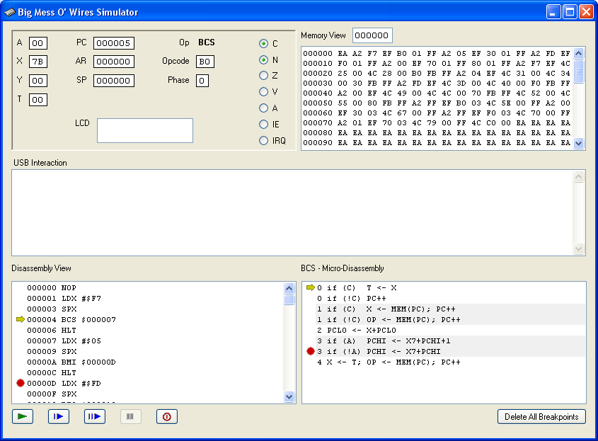
The top-left panel shows the current state of the registers and condition codes, as well as the current opcode, instruction, and phase (the index of the current micro-instruction). Eventually this area will also show the current state of the LCD.
The top-right is a standard memory view. Just type in the base address of the region of memory to examine.
At the bottom-left is the source view. This shows a disassembly of the program boot ROM, in the area near the PC. Yes, I wrote a BMOW-6502 disassembler to generate the source for this view. The current instruction is shown with a yellow arrow, and you can set breakpoints by clicking in the margin to the left of an instruction, just like in Visual Studio.
The bottom-right is the microcode source view. It shows a micro-disassembly (yes, I wrote a second disassembler) of the instruction currently being executed in the source view. The microinstructions in each phase are shaded the same color, to make it easier to visualize the groupings. Only one microinstruction from each phase will get executed, depending on the state of the condition codes at the time of execution.
Breakpoints can be set in the microcode too. Here you can see I set a breakpoint within BCS (branch if carry set) for the case where the branch is taken but the address arithmetic doesn’t generate an address carry when adding the branch offset to the PC. This is really cool, in my not-so-disinterested opinion.
Be the first to comment!